Fingerprint recognition device and control method, touch display panel, touch display device

A touch display panel and fingerprint recognition technology, applied in the touch display device, fingerprint recognition device and control method, and touch display panel field, can solve problems such as difficult fingerprint recognition, and achieve the effect of improving the recognition difference and improving the recognition accuracy.

Active Publication Date: 2018-06-15
BOE TECH GRP CO LTD
View PDF4 Cites 1 Cited by
  • Summary
  • Abstract
  • Description
  • Claims
  • Application Information

AI Technical Summary

Problems solved by technology

[0005] Aiming at the problem that the existing liquid crystal display is difficult to accurately identify fingerprints, the present invention provides a fingerprint identification device, a touch display panel, a touch display device and a control method for the fingerprint identification device

Method used


Image

  • Fingerprint recognition device and control method, touch display panel, touch display device
  • Fingerprint recognition device and control method, touch display panel, touch display device
  • Fingerprint recognition device and control method, touch display panel, touch display device

Examples


Embodiment 1

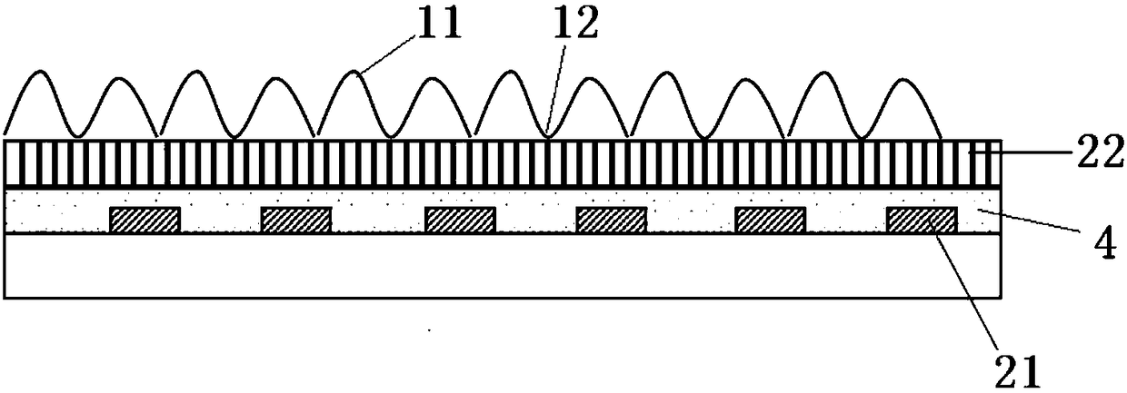
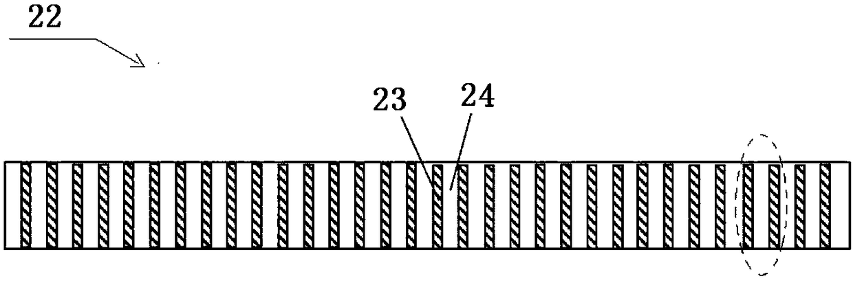
[0037] This embodiment provides a fingerprint identification device, such as Figure 2-4 As shown, it includes: a photoelectric sensor 21 and an optical waveguide structure 22; the optical waveguide structure 22 is used to be arranged on the touch substrate to contact with the fingerprint. The optical waveguide structure 22 includes a dielectric material 23 and a waveguide material 24 arranged at intervals, and the sides of the dielectric material 23 and the waveguide material 24 away from the touch substrate 4 are both used for contacting with fingerprints, so as to inject light from the touch substrate 4 into the waveguide. The light from the material 24 propagates to the surface of the waveguide material 24 away from the touch substrate 4 after total reflection at the interface between the dielectric material 23 and the waveguide material 24 .

[0038] Specifically, such as figure 2 The fingerprint identification device shown includes a photoelectric sensor 21 disposed in...

Embodiment 2

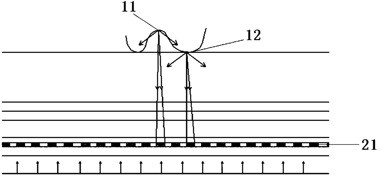
[0040] This embodiment provides a fingerprint identification device, including: a photoelectric sensor 21 and an optical waveguide structure 22 for contacting with a fingerprint on the touch substrate 4; the optical waveguide structure 22 includes a dielectric material 23 and a waveguide material 24 arranged at intervals , wherein, the interface between the waveguide material 24 and the touch substrate 4 is the first interface, the interfaces between the waveguide material 24 and the two adjacent dielectric materials 23 are respectively the second interface and the third interface, and the waveguide material 24 The surface far away from the touch substrate 4 is the fourth interface; the fourth interface is used to contact the fingerprint, so that the light incident on the waveguide material 24 from the first interface is transmitted to the second interface and the third interface after multiple times of total reflection. On the four interfaces;

[0041]When the trough 11 of th...

Embodiment 3

[0059] This embodiment provides a touch display panel, such as Figure 9 As shown, it includes the above-mentioned fingerprint identification device, and also includes a touch display substrate, the optical waveguide structure 22 is arranged on the touch display surface of the touch display substrate, and the photoelectric sensor 21 is arranged on the touch display substrate away from the optical waveguide. One side of structure 22.

[0060] That is to say, the touch substrate 4 in this embodiment is a touch display substrate. Here, a liquid crystal touch display substrate is used as an example for illustration. See Figure 9 The liquid crystal layer 3 is between the color filter substrate 31 and the array substrate 32, the optical waveguide structure 22 is arranged on the color filter substrate 31, the photoelectric sensor 21 is arranged on the side of the array substrate 31 close to the color filter substrate 32, and the light from the backlight 33 After being injected from...


PUM


Abstract

The invention provides a fingerprint identification device, a touch display panel and a control method for fingerprint identification, which belong to the field of display technology and can solve the problem that the existing liquid crystal display is difficult to accurately identify fingerprints. The fingerprint identification device of the present invention includes a photoelectric sensor and an optical waveguide structure, the optical waveguide structure includes a dielectric material and a waveguide material that are vertically spaced apart, after the light is injected into the waveguide material, it is totally reflected at the interface between the dielectric material and the waveguide material and propagates to The waveguide material is away from the face of the touch substrate. If the trough of the fingerprint is in contact with the surface, since the trough is air, the light is totally reflected and returned to be recognized by the photoelectric sensor; if the ridge of the fingerprint is in contact with the surface, the diffuse reflection of light at the ridge will not be recognized by the photoelectric sensor, which is quite It improves the recognition difference between the ridge and the trough, thereby improving the recognition accuracy of the photoelectric sensor for the trough and the ridge. The fingerprint identification device of the present invention is suitable for various display devices.

Description

technical field [0001] The invention belongs to the field of display technology, and in particular relates to a fingerprint identification device and a control method, a touch display panel, and a touch display device. Background technique [0002] Nowadays, fingerprint recognition technology has been widely used in many fields, such as mobile phones, tablet computers and TVs in electronic equipment terminals; access control and safes in security protection systems, etc. The realization methods of fingerprint collection mainly include optical, capacitive and ultrasonic imaging technologies, among which the optical fingerprint recognition technology has a relatively large recognition range and relatively low cost. [0003] At present, the optical fingerprint identification technology used in mobile terminals such as mobile phones is not yet mature, and in the prior art, the backlight is used to illuminate the finger, and the finger diffusely reflects the light beam to the pho...

Claims


Application Information

Patent Timeline
Patent Type & Authority Patents(China)
IPC IPC(8): G06K9/00G02B6/08G02B6/26G06F3/041
CPCG06F3/0412G02B6/08G02B6/262G06V40/1324H01L27/14678G06F3/0421G06F2203/04109H10K59/65H01L27/14621H01L27/14629G06V40/1318H10K50/84H10K59/38
Inventor 谭纪风杨亚锋
Owner BOE TECH GRP CO LTD
Why Eureka
Try Eureka