Guidable FPGA (field programmable gate array) configuration circuit

A technology for configuring circuits and configuring information, applied in the direction of boot program, program control device, electrical digital data processing, etc., can solve the problems of small storage information capacity, power failure processing, troublesome use, etc., and achieve the effect of reducing the number of chips

Active Publication Date: 2017-07-11
XIDIAN UNIV
View PDF3 Cites 4 Cited by
  • Summary
  • Abstract
  • Description
  • Claims
  • Application Information

AI Technical Summary

Problems solved by technology

[0003] To sum up, the problems existing in the prior art are: the existing FPGA has a small capacity for storing information, and multiple chips are required to store multiple copies of FPGA configuration information; moreover, power outage processing is required for information configuration, which is cumbersome to use

Method used


Image

  • Guidable FPGA (field programmable gate array) configuration circuit

Examples


Embodiment Construction

[0009] In order to further understand the content, features and effects of the present invention, the following examples are given, and detailed descriptions are given below with reference to the accompanying drawings.

[0010] The structure of the present invention will be described in detail below in conjunction with the accompanying drawings.

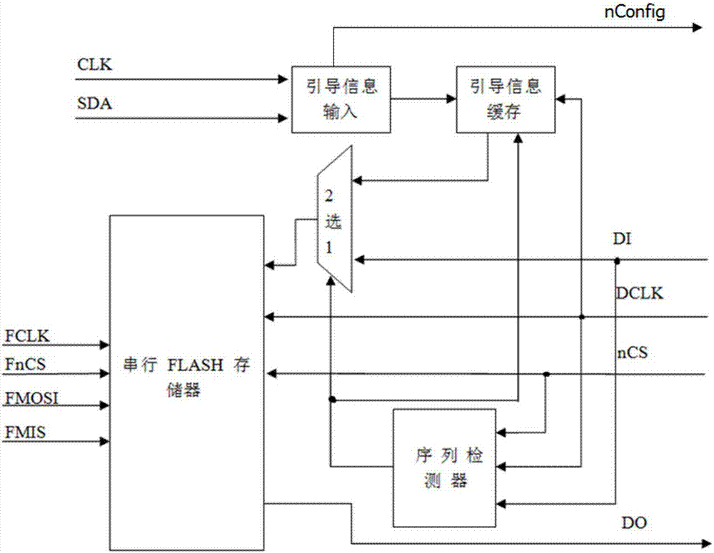
[0011] Such as figure 1 As shown, the bootable FPGA configuration circuit provided by the embodiment of the present invention includes a serial FLASH memory, and the FCLK, FnCS, FMOSI, and FMIS interfaces of the serial FLASH memory are connected to an external processor; the configuration information is written to the serial FLASH through the above-mentioned interface Memory; interface CLK, SDA to connect to external processor; set boot information through the above interface; nConfig, DI, DCLK, nCS, DO connect to FPGA through wires.

[0012] Further, the data writing of the serial FLASH memory: the external processor finishes writi...


PUM


Abstract

The invention belongs to the technical field of design and development of circuits, and discloses a guidable FPGA (field programmable gate array) configuration circuit. The guidable FPGA configuration circuit comprises a serial FLASH memory, wherein FCLK, FnCS, FMOSI and FMIS interfaces of the serial FLASH memory are connected with an external processor; the configuration information is written into the serial FLASH memory via the interfaces; CLK and SNA interfaces are connected with the external processor; the guiding information is set via the interfaces; nConfig, DI, DCLK, nCS and DO are connected with the FPGA. The guidable FPGA configuration circuit has the advantages that if the capacity of the FLASH memory is enough, multiple copies of FPGA configuration information can be stored in one FLASH chip, so that the number of chips can be reduced; the external processor can force the FPGA to reconfigure via CLK and SDA, so as to realize the heat exchange of the FPGA functions.

Description

technical field [0001] The invention belongs to the technical field of circuit design and development, in particular to a bootable FPGA configuration circuit. Background technique [0002] At present, when the existing FPGA is powered on, the configuration information of the FPGA is read from an external EPCS device through a specific interface to complete the configuration of the FPGA. Therefore, when the logic of the FPGA needs to be changed, the external EPCS needs to be reprogrammed to complete the configuration process. Moreover, only one copy of FPGA configuration information is saved for an EPCS chip with sufficient capacity. [0003] To sum up, the existing technology has the following problems: the existing FPGA has a small capacity for storing information, and multiple chips are required to store multiple copies of FPGA configuration information; moreover, power outage processing is required for information configuration, which is cumbersome to use. Contents of ...

Claims


Application Information

Patent Timeline
Patent Type & Authority Applications(China)
IPC IPC(8): G06F9/44G06F13/40
CPCG06F9/4401G06F13/4068
Inventor 任爱锋吴治斌
Owner XIDIAN UNIV
Why Eureka
Try Eureka