Micro-component transfer device, transfer method, manufacturing method, device, and electronic device

A transfer device and transfer method technology, applied in semiconductor/solid-state device manufacturing, measuring devices, electrical components, etc.

Active Publication Date: 2017-08-11
XIAMEN SANAN OPTOELECTRONICS TECH CO LTD
View PDF3 Cites 60 Cited by
  • Summary
  • Abstract
  • Description
  • Claims
  • Application Information

AI Technical Summary

Problems solved by technology

One of the difficulties in the fabrication of microcomponents is how to tran

Method used


Image

  • Micro-component transfer device, transfer method, manufacturing method, device, and electronic device
  • Micro-component transfer device, transfer method, manufacturing method, device, and electronic device
  • Micro-component transfer device, transfer method, manufacturing method, device, and electronic device

Examples


specific Embodiment

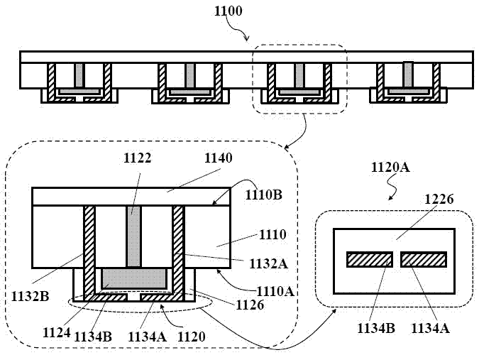
[0086] figure 1 A cross-sectional side view of a transfer device according to a first preferred embodiment of the present invention is shown. The transfer device 1100 includes: a base substrate 1110 , an array of pick-up heads 1120 , a testing circuit and a CMOS integrated circuit 1140 . Specifically, the base substrate 1110 is used to provide a supporting function, and may be formed of various materials, such as silicon, ceramics, and polymers. The pick-up heads 1120 are arranged in an array on the first surface 1110A of the base substrate 1110, with a size ranging from 1 μm to 100 μm, for example, 50 μm to 20 μm, and a pitch of (1 μm to 100 μm)×(1 μm to 100 μm), for example 10μm x 10μm or 50μm x 100μm pitch. The array of pick-up heads 1120 is disposed on the first surface 1110A of the base substrate 1100 for picking up micro-components by various adsorption forces (such as electrostatic force, vacuum pressure, van der Waals force, magnetic force, etc.) to achieve the funct...


PUM

PropertyMeasurementUnit
Thicknessaaaaaaaaaa
Radiusaaaaaaaaaa

Abstract

The invention discloses a micro-component transfer device, a transfer method, a manufacturing method, a device and an electronic device. According to the invention, when micro-components are being transferred, testing can be done to the micro-components so as to remove the micro-components with defects. The micro-component transfer device with a testing circuit comprises a base substrate with two opposite surfaces; a pick-up head array formed on the first surface of the base substrate and used to pick up or release the micro-components; and a testing circuit arranged inside of the base substrate or the surface of the base substrate and consisting of a series of sub-testing circuits with each sub-testing circuit containing at least two testing electrodes and used to test the optical-electro parameters of the micro-components when the micro-components are being transferred by the transfer device.

Description

technical field [0001] The present invention relates to a micro-element for display, and more particularly, to a transfer device, a transfer method, a manufacturing method, a device and an electronic device for a micro-element. Background technique [0002] Micro-component technology refers to an array of micro-sized components integrated at high density on a substrate. At present, micro-pitch light-emitting diode (Micro LED) technology has gradually become a research hotspot, and the industry expects high-quality micro-component products to enter the market. High-quality fine-pitch light-emitting diode products will have a profound impact on traditional display products such as LCD / OLED that are already on the market. [0003] In the process of fabricating microcomponents, the microcomponents are first formed on a donor substrate and then transferred to a receiving substrate. The receiving substrate is, for example, a display screen. One difficulty in the fabrication of ...

Claims


Application Information

Patent Timeline
IPC IPC(8): H01L21/66H01L21/67H01L21/683
CPCH01L21/67271H01L21/683H01L22/14H01L21/6838H01L21/6831G01R31/2887H01L33/0095H01L33/62H01L25/0753H01L2224/95H01L21/67288H01L22/34H01L24/00
Inventor 徐宸科邵小娟郑建森其他发明人请求不公开姓名
Owner XIAMEN SANAN OPTOELECTRONICS TECH CO LTD
Why Eureka
Try Eureka