Array substrate, display panel and display device

An array substrate and substrate substrate technology, which is applied to instruments, computing, electrical digital data processing, etc., can solve the problems of coupling capacitances that cannot cancel each other, signal crosstalk of liquid crystal display panels, and affect the display effect of liquid crystal display panels, etc., to eliminate the signal Crosstalk, the effect of improving the display effect

Active Publication Date: 2020-04-14
XIAMEN TIANMA MICRO ELECTRONICS
View PDF3 Cites 0 Cited by
  • Summary
  • Abstract
  • Description
  • Claims
  • Application Information

AI Technical Summary

Problems solved by technology

During the display period, around the opening, in the same pixel unit, the coupling capacitance formed by the pixel electrode and the data lines on both sides is not equal. In the column inversion driving mode, the coupling capacitance formed by the pixel electrode and the data lines on both sides cannot Offset each other, and the LCD panel has signal crosstalk, which affects the display effect of the LCD panel

Method used


Image

  • Array substrate, display panel and display device
  • Array substrate, display panel and display device
  • Array substrate, display panel and display device

Examples


Embodiment Construction

[0044] The present invention will be further described in detail below in conjunction with the accompanying drawings and embodiments. It should be understood that the specific embodiments described here are only used to explain the present invention, but not to limit the present invention. In addition, it should be noted that, for the convenience of description, only some structures related to the present invention are shown in the drawings but not all structures.

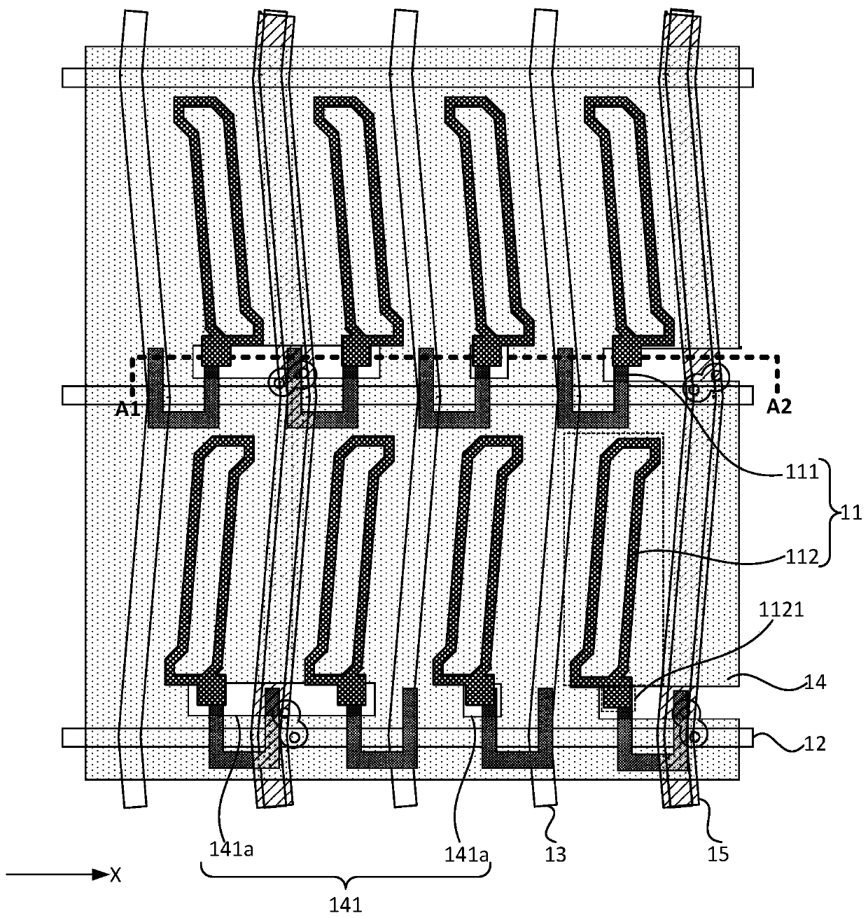
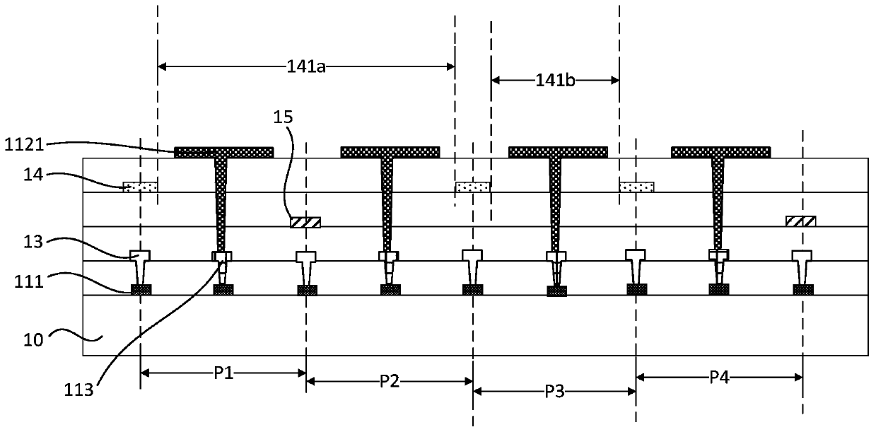
[0045] Figure 1a It is a structural schematic diagram of an array substrate in an existing liquid crystal display panel, Figure 1b for along Figure 1a Schematic diagram of the cross-sectional structure of A1-A2. see Figure 1a with Figure 1b The array substrate includes a base substrate 10, a plurality of pixel units 11 formed on the base substrate 10, a plurality of scanning lines 12 and a plurality of data lines 13, and a plurality of touch electrodes 14 arranged in an array ( Figure 1a Only one touch elec...


PUM


Abstract

Embodiments of the invention disclose an array substrate, a display panel and a display device. The array substrate comprises a substrate, a plurality of pixel units, a plurality of scanning lines, a plurality of data lines, a plurality of touch electrodes, a plurality of touch lines, a plurality of pixel areas and a plurality of compensation lines, wherein each of the pixel units comprises a thin-film transistor and a pixel electrode; a plurality of openings are formed in the touch electrodes; the projection, on the substrate, of the joints of the pixel electrodes and the drain electrodes of the thin-film transistors are located in the projections, on the substrate, of the openings; the plurality of compensation lines and the plurality of touch lines are arranged on the same layer; the plurality of compensation lines are electrically connected with the adjacent touch electrodes; the compensation lines cover a part of the areas, not covered by the touch lines, of the data lines; and in the pixel areas, the touch lines and the compensation lines are located at two opposite sides of the joints of the pixel electrodes and the drain electrodes of the thin-film transistors. By utilizing the array substrate provided by the embodiments of the invention, the display effect of liquid crystal display panels can be improved.

Description

technical field [0001] Embodiments of the present invention relate to liquid crystal display technology, and in particular to an array substrate, a display panel and a display device. Background technique [0002] Liquid crystal display panel is a display panel made of liquid crystal material. It has the characteristics of light and thin, low power consumption and large amount of displayed information. It is widely used in mobile phones, TVs, computers, smart wearable devices and information inquiry machines in public halls, etc. . [0003] Existing liquid crystal display panels often include a plurality of pixel units, a plurality of data lines, a plurality of touch control lines and a plurality of touch electrodes arranged in an array. The pixel unit includes a thin film transistor and a pixel electrode. Multiple touch traces cover part of the data lines. Each touch electrode is electrically connected to at least one touch trace. Usually, a plurality of openings are pr...

Claims


Application Information

Patent Timeline
Patent Type & Authority Patents(China)
IPC IPC(8): G06F3/044G06F3/041G02F1/1362G02F1/1333
CPCG02F1/13338G02F1/136286G06F3/0412G06F3/044
Inventor 吴昊
Owner XIAMEN TIANMA MICRO ELECTRONICS
Why Eureka
Try Eureka