
High-speed transmission optical module circuit board structure, manufacturing method, and crosstalk prevention method

A high-speed transmission and circuit board technology, which is applied to printed circuits, circuit heating devices, printed circuit components, etc., can solve problems such as heat generation and small printed circuit boards that cannot obtain sufficient mechanical strength

Active Publication Date: 2020-12-29
SHENZHEN OPTIC KING TECH
View PDF4 Cites 0 Cited by
  • Summary
  • Abstract
  • Description
  • Claims
  • Application Information

AI Technical Summary

Problems solved by technology

In addition to the differential signal line pair buried in the blind hole, the first signal transmission layer (top differential signal line) is connected to the gold finger on the top layer, and the second signal transmission layer (bottom surface differential signal line) is connected to the bottom gold finger. It helps to avoid the concentrated crosstalk between the differential signal lines on the first signal transmission layer and the differential signal line pairs on the second signal transmission layer; the differential signal lines on the surface are located in the hollow pattern of the ground plane of the same layer, which is very important for the optical module The small printed circuit boards used do not have sufficient mechanical strength, and the problem of layer peeling due to heat generation during the operation of high-transmission optical modules is prone to occur

Method used


Image

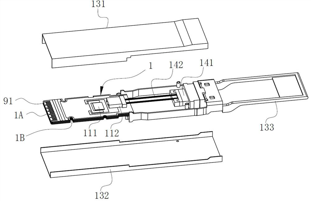
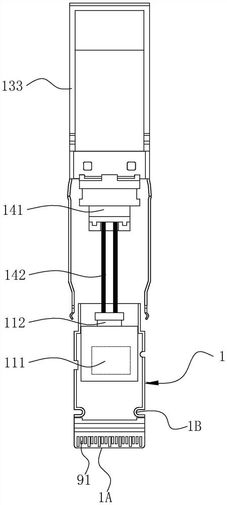
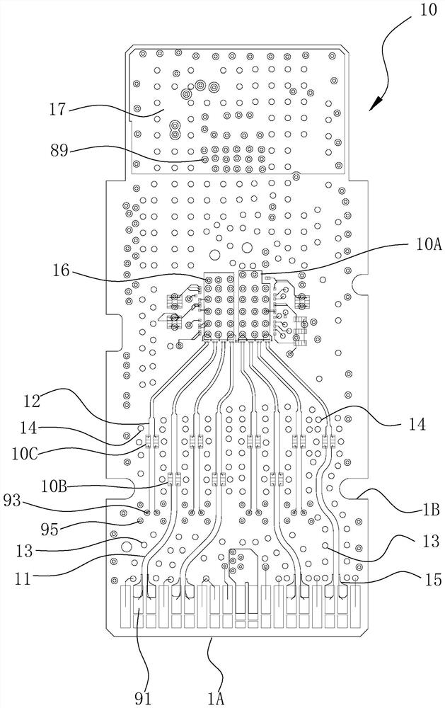
  • High-speed transmission optical module circuit board structure, manufacturing method, and crosstalk prevention method
  • High-speed transmission optical module circuit board structure, manufacturing method, and crosstalk prevention method
  • High-speed transmission optical module circuit board structure, manufacturing method, and crosstalk prevention method

Examples


Embodiment Construction

[0060] The technical solutions in the embodiments of the present invention will be clearly and completely described below in conjunction with the accompanying drawings in the embodiments of the present invention. Apparently, the described embodiments are only part of the embodiments for understanding the inventive concepts of the present invention, and cannot represent All the embodiments are not explained as the only embodiment. Based on the embodiments of the present invention, all other embodiments obtained by persons of ordinary skill in the art on the premise of understanding the inventive concepts of the present invention fall within the protection scope of the present invention.

[0061] It should be noted that if there is a directional indication (such as up, down, left, right, front, back...) in the embodiment of the present invention, the directional indication is only used to explain the position in a certain posture (as shown in the accompanying drawing). If the sp...


PUM


Abstract

It relates to a high-speed transmission optical module circuit board structure, its manufacturing method, and a crosstalk prevention method. In order to effectively integrate and isolate differential signal lines in the high-speed transmission optical module, the circuit board structure includes a multi-layer circuit laminate, which is arranged on both sides of the plug-in side The row contact means that the multi-layer circuit laminate includes a transmission signal layer, a control signal layer, a power signal layer and an integrated circuit layer for partition management separated by an isolation layer, and a pair of first differential signal lines and a pair of second differential signal lines. The first segment of the differential signal line is located in the transmission signal layer, and the first differential signal line is connected to the first row of contact fingers; the second segment of the second differential signal line is located in the first area of ​​the integrated circuit layer and connected to the corresponding second row Contact fingers; electrically connect the first section and the second section of the second differential signal line with long connection via holes; electrically connect the rest of the second row of contact fingers to the corresponding control signal layer and power signal layer with short connection via holes ; The integrated circuit layer also includes the power line connection section, the control line connection section and the ground cooling island located in the second area.

Description

technical field [0001] The invention relates to the technical field of internal devices of high-speed transmission optical modules, in particular to a high-speed transmission optical module circuit board structure, a manufacturing method thereof, and a crosstalk prevention method. Background technique [0002] High-speed transmission optical modules, such as single / dual-fiber pluggable optical modules (SFP) are small pluggable transceiver devices that contain active chips and optical receiving transmitters. They are used in high-speed telecommunications and data communications. In order to match 5G, 6G or Under more advanced communication protocols, the amount of data that needs to be transmitted within a limited time is also increasing, and the transmission rate is increased to 100 Gb / s or higher. In order to correct / correct the distortion or delay of data data at high transmission rates, the circuit board Differential signal lines are used in the structure for high-speed d...

Claims


Application Information

Patent Timeline
Patent Type & Authority Patents(China)
IPC IPC(8): H05K1/02G02B6/42
CPCG02B6/428H05K1/0209H05K1/0228H05K1/0245H05K1/0271
Inventor 刘萍刘平周俊文彭彦辉刘斌
Owner SHENZHEN OPTIC KING TECH
Features
  • Generate Ideas
  • Intellectual Property
  • Life Sciences
  • Materials
  • Tech Scout
  • Unparalleled Data Quality
  • Higher Quality Content
  • 60% Fewer Hallucinations
Learn More