Methods of manufacturing an image sensor having an air gap

an image sensor and air gap technology, applied in the direction of electrical equipment, semiconductor devices, radio frequency control devices, etc., can solve the problems of black-and-white image sensor image distortion, black-and-white image sensor image loss, tint failure, etc., and achieve the effect of preventing metal loss

Active Publication Date: 2010-08-12
SAMSUNG ELECTRONICS CO LTD
View PDF10 Cites 39 Cited by
  • Summary
  • Abstract
  • Description
  • Claims
  • Application Information

AI Technical Summary

Benefits of technology

[0018]Removing the ILD may include forming a hard mask formed of SiN on the reflection pattern,

Problems solved by technology

However, in the case of the image sensor, the generated photocharges may be transmitted to and accumulated in a photoelectric conversion device of an adjacent pixel, thereby causing crosstalk between the pixels.
When crosstalk occurs, a black-and-white image sensor may suffer from image distortion due to its low resolution.
Also,

Method used


Image

  • Methods of manufacturing an image sensor having an air gap
  • Methods of manufacturing an image sensor having an air gap
  • Methods of manufacturing an image sensor having an air gap

Examples


Embodiment Construction

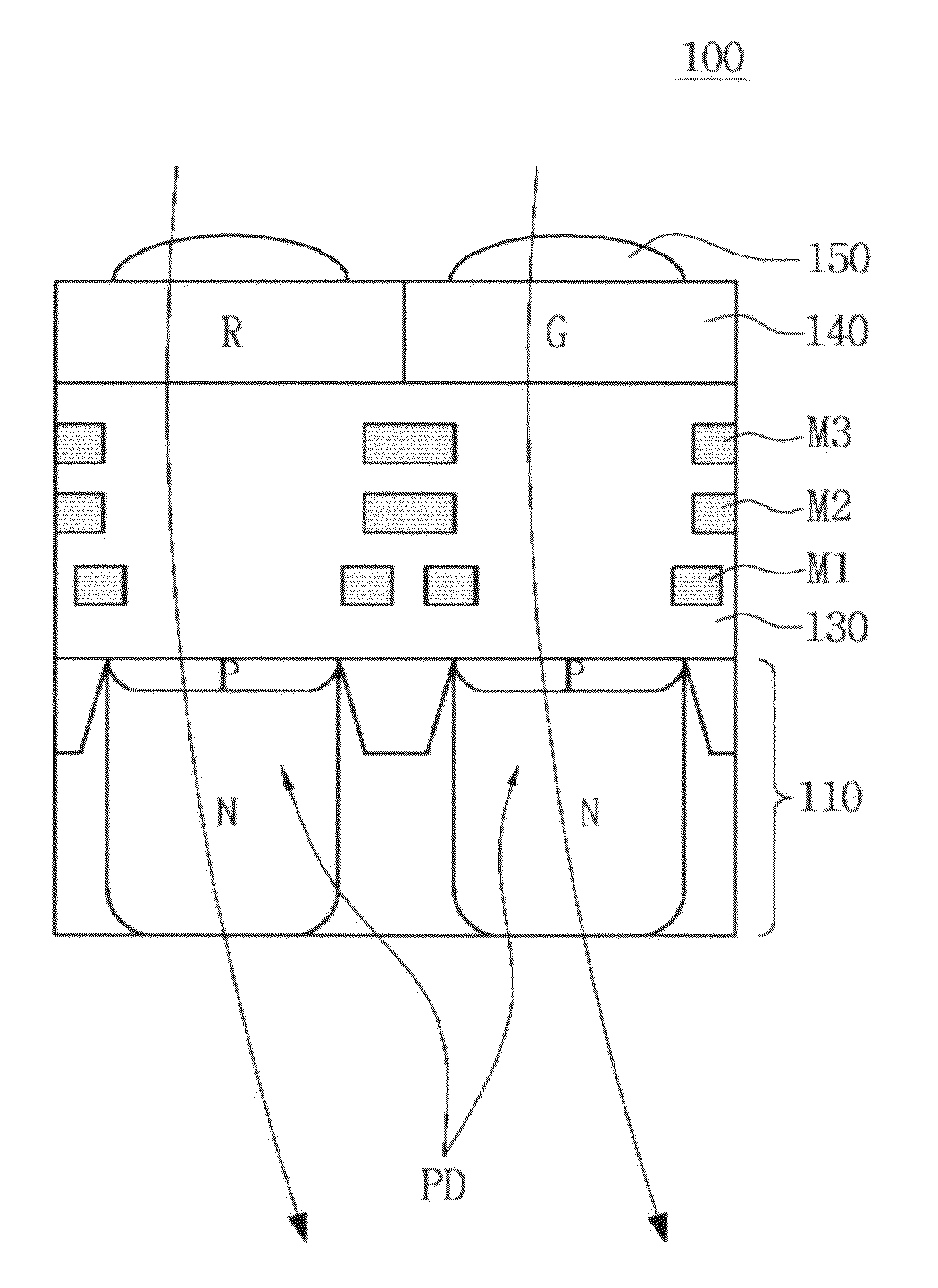
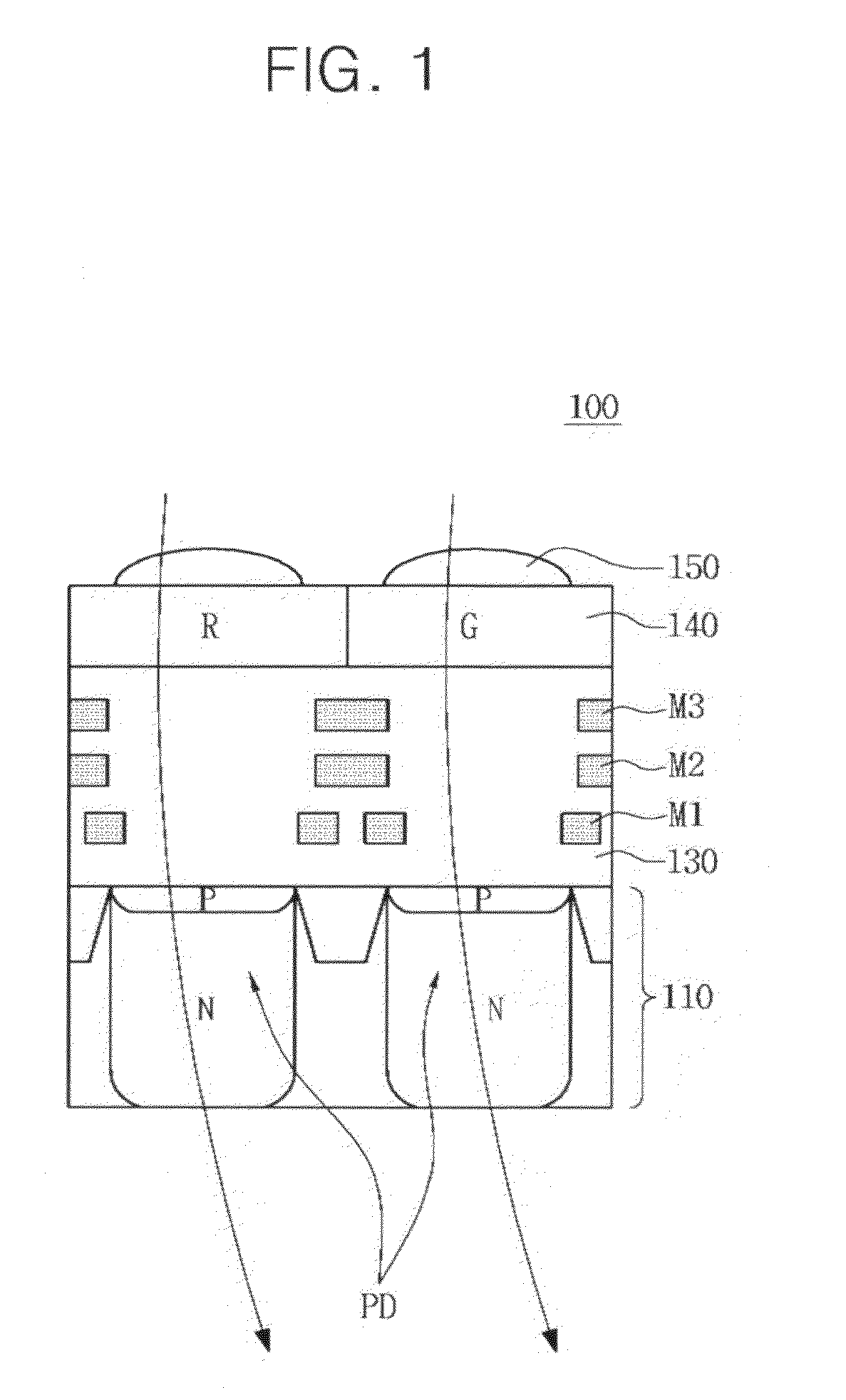
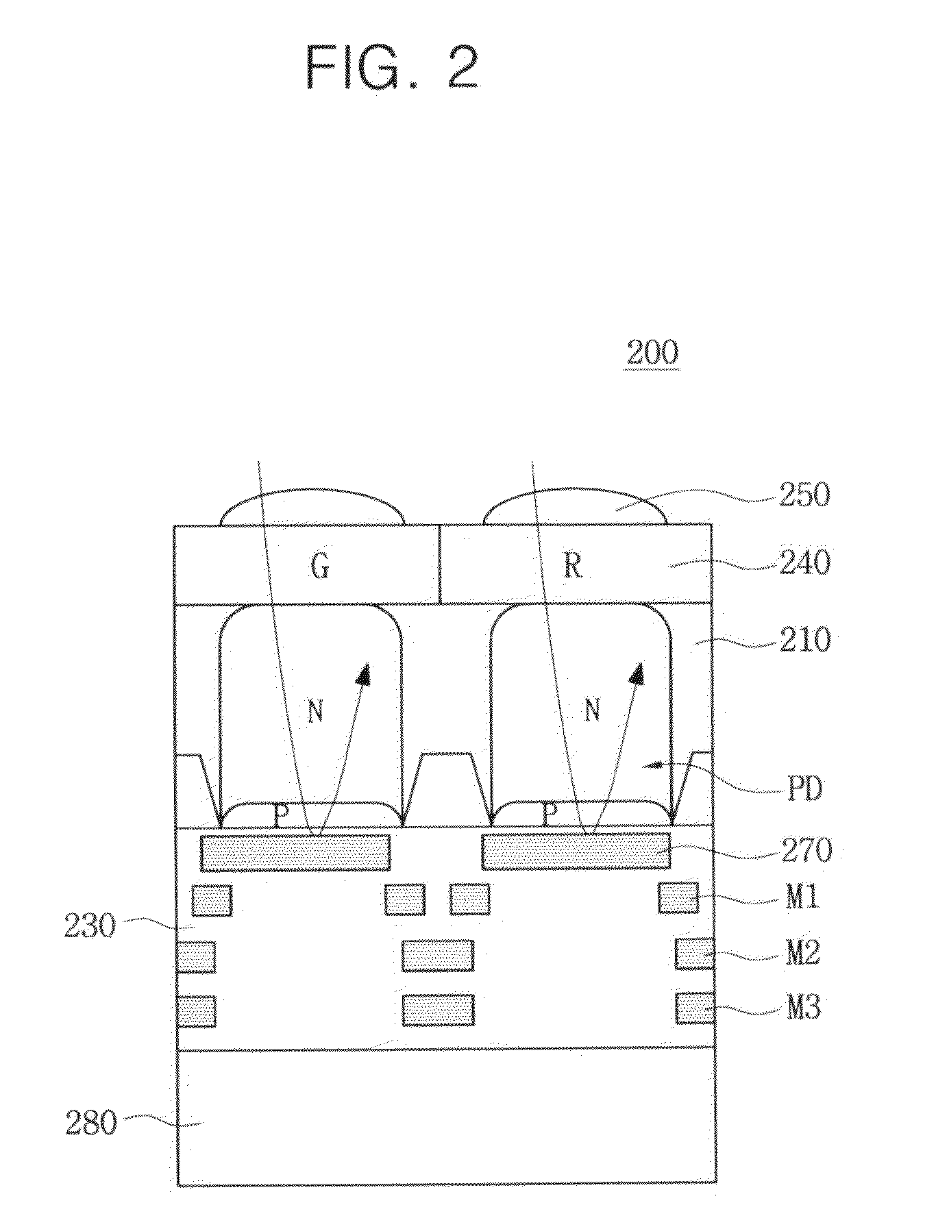
[0044]Example embodiments of the present invention will be more clearly understood from the detailed description taken in conjunction with the accompanying drawings.

[0045]Various example embodiments of the present invention will now be described more fully with reference to the accompanying drawings in which some example embodiments of the invention are shown. In the drawings, the thicknesses of layers and regions may be exaggerated for clarity.

[0046]Detailed illustrative embodiments of the present invention are disclosed herein. However, specific structural and functional details disclosed herein are merely representative for purposes of describing example embodiments of the present invention. This invention may, however, may be embodied in many alternate forms and should not be construed as limited to only the embodiments set forth herein.

[0047]Accordingly, while example embodiments of the invention are capable of various modifications and alternative forms, embodiments thereof ar...


PUM


Abstract

In an example embodiment, the method of manufacturing an image sensor includes forming an interlayer dielectric (ILD) on a substrate. The substrate may have a plurality of pixels arranged thereon and each of the pixels includes a photoelectric conversion device configured to sense external light and generate photo charges. Furthermore, the method may include forming a metal on the ILD and removing portions of the metal to form a reflection pattern. Additionally, the method may include removing the ILD to a depth to form a trench adjacent to the reflection pattern and forming an air gap in the trench by forming oxide over the substrate such that the reflection pattern and the upper portion of the trench are covered.

Description

CROSS-REFERENCE TO RELATED APPLICATION[0001]This application claims the benefit of priority under 35 U.S.C. §119 from Korean Patent Application No. 10-2009-0010345, filed on Feb. 9, 2009, the disclosure of which is hereby incorporated herein by reference in its entirety by reference.BACKGROUND[0002]1. Field[0003]Example embodiments relate to a method of manufacturing an image sensor having an air gap, and more particularly, to a method of manufacturing a back-illuminated image sensor in which a light receiving unit is formed on a rear surface. Example embodiments further relate to a method of manufacturing an image sensor in which a reflection pattern is formed on a dielectric layer to improve optical sensitivity of a light receiving unit formed on a rear surface. Additional embodiments relate to a method of manufacturing an image sensor in which a reflection pattern is formed simultaneously with an interconnection pattern. Other embodiments relate to a method of manufacturing an im...

Claims


Application Information

Patent Timeline
IPC IPC(8): H01L31/18H01L31/0232
CPCH01L27/14627H01L27/14632H01L27/14689H01L27/14685H01L27/14645H01L27/146
Inventor PARK, BYUNG-JUN
Owner SAMSUNG ELECTRONICS CO LTD
Why Eureka
Try Eureka