A Planar Torsion Microsensor for High Magnetic Field Measurement
A twisting micro sensor technology, applied in the direction of the magnitude/direction of the magnetic field, measuring devices, measuring magnetic variables, etc., can solve problems such as poor radiation resistance, reduced sensor quality factor, unsuitable for Tokamak high temperature, strong radiation environment, etc.
- Summary
- Abstract
- Description
- Claims
- Application Information
AI Technical Summary
Problems solved by technology
Method used
Image
Examples
Embodiment 1
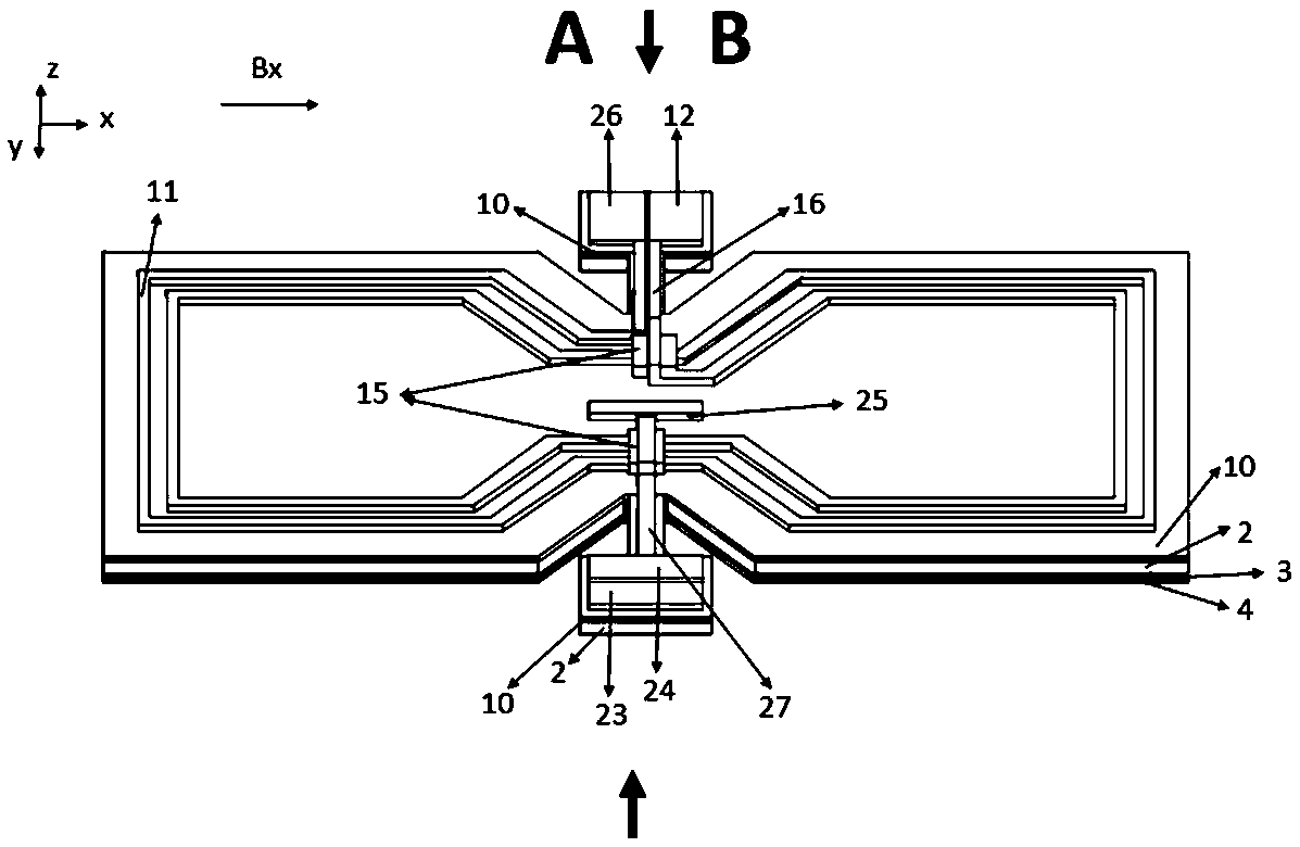
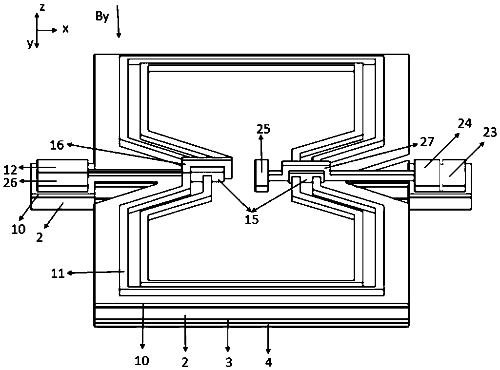
[0050] A planar torsion microsensor for measuring a strong magnetic field includes a substrate, a sensor body and a cover that are sequentially connected.
[0051] The substrate is a single-sided polished wafer 5 with a thickness of 500 um, a cavity with a depth of 1.2 um is provided on the polished side, and a first silicon oxide layer 6 is provided on the entire polished surface with the cavity;
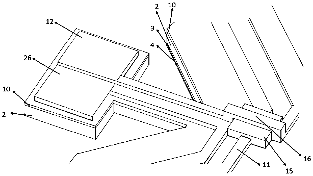
[0052] see figure 1 , the sensor body is prepared on the basis of SOI wafer 1, and the sensor body is divided into three parts: the coil electrode anchor area, the torsion plane, and the capacitive electrode anchor area; the length direction of the torsion plane is the X direction, the width direction is the Y direction, and the torsion plane The two sides of the middle part in the Y direction are respectively concave inward, the coil electrode anchor area is located outside one side of the Y direction in the middle of the torsion plane; the capacitive electrode anchor area is loca...
Embodiment 2
[0064] The steps to prepare the planar torsion microsensor for strong magnetic field measurement are as follows:
[0065] (1). On the side of the silicon material layer 2 of the SOI wafer 1 of the sensor body, use deep reactive ion etching technology to pattern-etch a cavity with a depth of 1um, and use lift-off technology to pattern-grow 400nm on the inner surface of the cavity respectively. The second silicon oxide layer 3 and the capacitor upper plate layer 4 . The material of the upper plate layer 4 of the capacitor is aluminum.
[0066] (2). On the single-sided polished wafer 5 of the substrate, a 1.2um deep cavity is etched using deep reactive ion etching technology, so that the single-sided polished wafer 5 has a "concave" shape, and after the cavity is etched A 400nm-thick first silicon oxide layer 6 is grown on the surface of the polished silicon material, and then an aluminum material is grown on the first silicon oxide layer 6 on the inner surface of the cavity as ...
PUM
 Abstract
Description
Claims
Application Information


