Planar torsional micro sensor for measurement of strong magnetic field
A torsional micro-sensor technology, applied in the size/direction of the magnetic field, measuring device, measuring magnetic variables, etc., can solve the problems of reduced sensor quality factor, poor radiation resistance, and large temperature dependence.
- Summary
- Abstract
- Description
- Claims
- Application Information
AI Technical Summary
Problems solved by technology
Method used
Image
Examples
Embodiment 1
[0050] A planar torsion microsensor for measuring a strong magnetic field includes a substrate, a sensor body and a cover that are sequentially connected.
[0051] The substrate is a single-sided polished wafer 5 with a thickness of 500 um, a cavity with a depth of 1.2 um is provided on the polished side, and a first silicon oxide layer 6 is provided on the entire polished surface with the cavity;
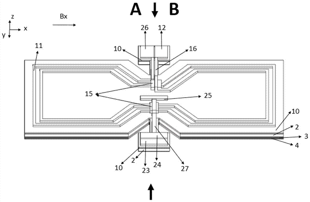
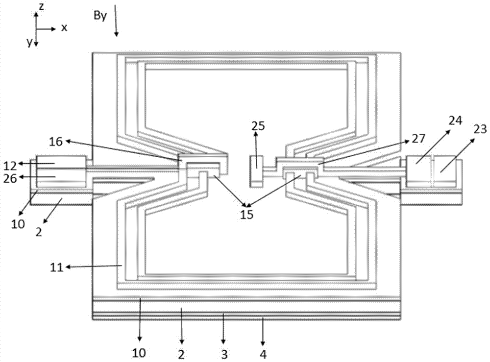
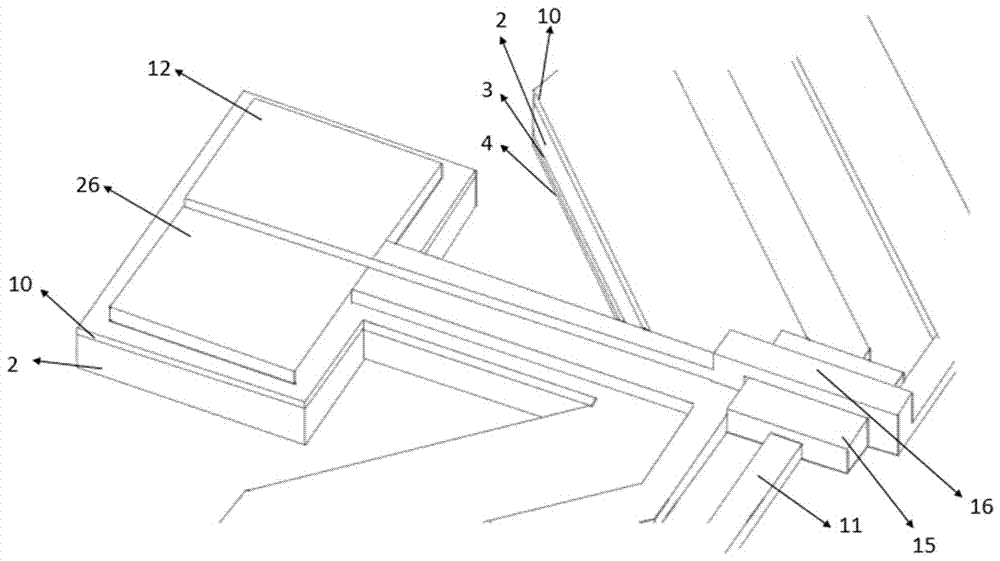
[0052] see figure 1 , the sensor body is prepared on the basis of SOI wafer 1, and the sensor body is divided into three parts: the coil electrode anchor area, the torsion plane, and the capacitive electrode anchor area; the length direction of the torsion plane is the X direction, the width direction is the Y direction, and the torsion plane The two sides of the middle part in the Y direction are respectively concave inward, the coil electrode anchor area is located outside one side of the Y direction in the middle of the torsion plane; the capacitive electrode anchor area is loca...
Embodiment 2
[0064] The steps to prepare the planar torsion microsensor for strong magnetic field measurement are as follows:
[0065] (1). On the side of the silicon material layer 2 of the SOI wafer 1 of the sensor body, use deep reactive ion etching technology to pattern-etch a cavity with a depth of 1um, and use lift-off technology to pattern-grow 400nm on the inner surface of the cavity respectively. The second silicon oxide layer 3 and the capacitor upper plate layer 4 . The material of the upper plate layer 4 of the capacitor is aluminum.
[0066] (2). On the single-sided polished wafer 5 of the substrate, a 1.2um deep cavity is etched using deep reactive ion etching technology, so that the single-sided polished wafer 5 has a "concave" shape, and after the cavity is etched A 400nm-thick first silicon oxide layer 6 is grown on the surface of the polished silicon material, and then an aluminum material is grown on the first silicon oxide layer 6 on the inner surface of the cavity as ...
PUM
 Abstract
Description
Claims
Application Information


