A method for adjusting the threshold of a cmos device and a cmos device

A device and threshold technology, applied in semiconductor devices, electrical solid state devices, semiconductor/solid state device manufacturing, etc., can solve the problems affecting the uniformity of small-sized metal gate filling and threshold control effect, NMOS and PMOS related parasitic effects, PMOS metal gate To solve the problems of complex laminated structure, it can improve filling uniformity and threshold control effect, reduce the influence of threshold adjustment correlation, and improve the accuracy of threshold control.

Active Publication Date: 2019-11-12
INST OF MICROELECTRONICS CHINESE ACAD OF SCI
View PDF5 Cites 0 Cited by
  • Summary
  • Abstract
  • Description
  • Claims
  • Application Information

AI Technical Summary

Problems solved by technology

[0003] The embodiment of the present application provides a method for adjusting the threshold of a CMOS device and a CMOS device, which solves the problem of the complex threshold adjustment process of CMOS devices in the prior art, the associated parasitic influence between NMOS and PMOS, the low accuracy of threshold control, and the low accuracy of PMOS metals. The gate stack structure is complex, which affects the filling uniformity and threshold control effect of small-sized metal gates

Method used


Image

  • A method for adjusting the threshold of a cmos device and a cmos device
  • A method for adjusting the threshold of a cmos device and a cmos device
  • A method for adjusting the threshold of a cmos device and a cmos device

Examples


Embodiment Construction

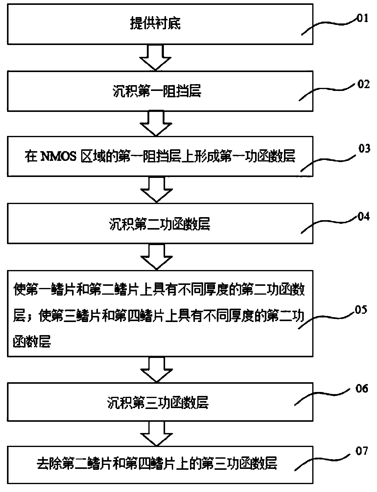
[0040] The embodiment of the present application provides a method for adjusting the threshold of a CMOS device and a CMOS device, which solves the problem of complex threshold adjustment process of CMOS devices in the prior art, the associated parasitic influence between NMOS and PMOS, low threshold control accuracy, and PMOS metal The gate stack structure is complex, which affects the filling uniformity and threshold control effect of small-sized metal gates.

[0041] The technical solution of the embodiment of the present application is to solve the above-mentioned technical problems, and the general idea is as follows:

[0042] A method of adjusting the threshold of a CMOS device, comprising:

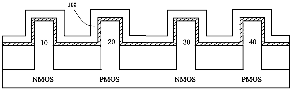
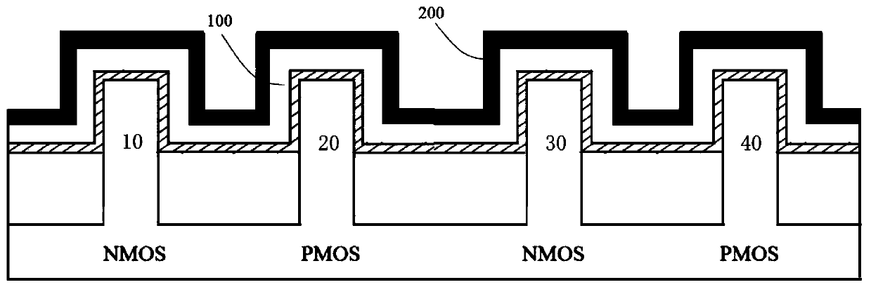
[0043] providing a substrate, the substrate including an NMOS region and a PMOS region, the NMOS region including a first fin and a second fin, and the PMOS region including a third fin and a fourth fin;

[0044] depositing a first barrier layer;

[0045] forming a first work func...


PUM


Abstract

The invention belongs to the technical field of a semiconductor and discloses a method for adjusting CMOS device threshold value and a CMOS device. The method comprises the following steps: providing a substrate; depositing a first barrier layer; forming a first work function layer in an NMOS region; depositing a second work function layer; enabling different fins in the NMOS and PMOS regions to have different thickness of second work function layers; depositing a third work function layer; and removing the third work function layer on the second and fourth fins. The device comprises the substrate, the first barrier layer, the first work function layer, the second work function layer and the third work function layer. The method solves the problems that the CMOS device threshold value adjusting process is complex, association parasitic influence occurs easily between NMOS and PMOS, threshold control precision is low and a device lamination structure is complex in the prior art, and achieves the technical effects of small threshold modulation association influence between the NMOS and PMOS and simple CMOS device lamination structure.

Description

technical field [0001] The invention relates to the technical field of semiconductors, in particular to a method for adjusting the threshold of a CMOS device and a CMOS device. Background technique [0002] The existing method for adjusting the threshold of CMOS devices is: the metal gates of NMOS and PMOS first deposit a barrier layer, then adjust the thickness of the barrier layer, then deposit a PMOS work function layer (PMOS WFL), and then change the thickness of the PMOS WFL to adjust the PMOS threshold; The NMOS work function layer (NMOS WFL) is deposited, and the NMOS WFL adjusts the NMOS threshold in combination with the thickness change of the previous barrier layer. Since the NMOS threshold adjustment process in this method needs to be divided into two stages, the CMOS device threshold adjustment process is complex, and the associated parasitic influence between NMOS and PMOS is easy to occur, which affects the accuracy of threshold control. In addition, the PMOS ...

Claims


Application Information

Patent Timeline
Patent Type & Authority Patents(China)
IPC IPC(8): H01L21/8238H01L27/092
CPCH01L21/823821H01L27/0924
Inventor 殷华湘张青竹赵超叶甜春
Owner INST OF MICROELECTRONICS CHINESE ACAD OF SCI
Why Eureka
Try Eureka