Glucose quantitative test sensor and preparation method based on microwave patch resonator
A chip resonator and resonator technology, applied in the direction of instruments, measuring devices, scientific instruments, etc., can solve the problems that limit the wide application of glucose biosensors, the accuracy and reliability of the results cannot be guaranteed, and achieve the benefits of commercial The effects of popularizing and applying, achieving reusability, and solving inaccuracy problems
- Summary
- Abstract
- Description
- Claims
- Application Information
AI Technical Summary
Problems solved by technology
Method used
Image
Examples
Embodiment 1
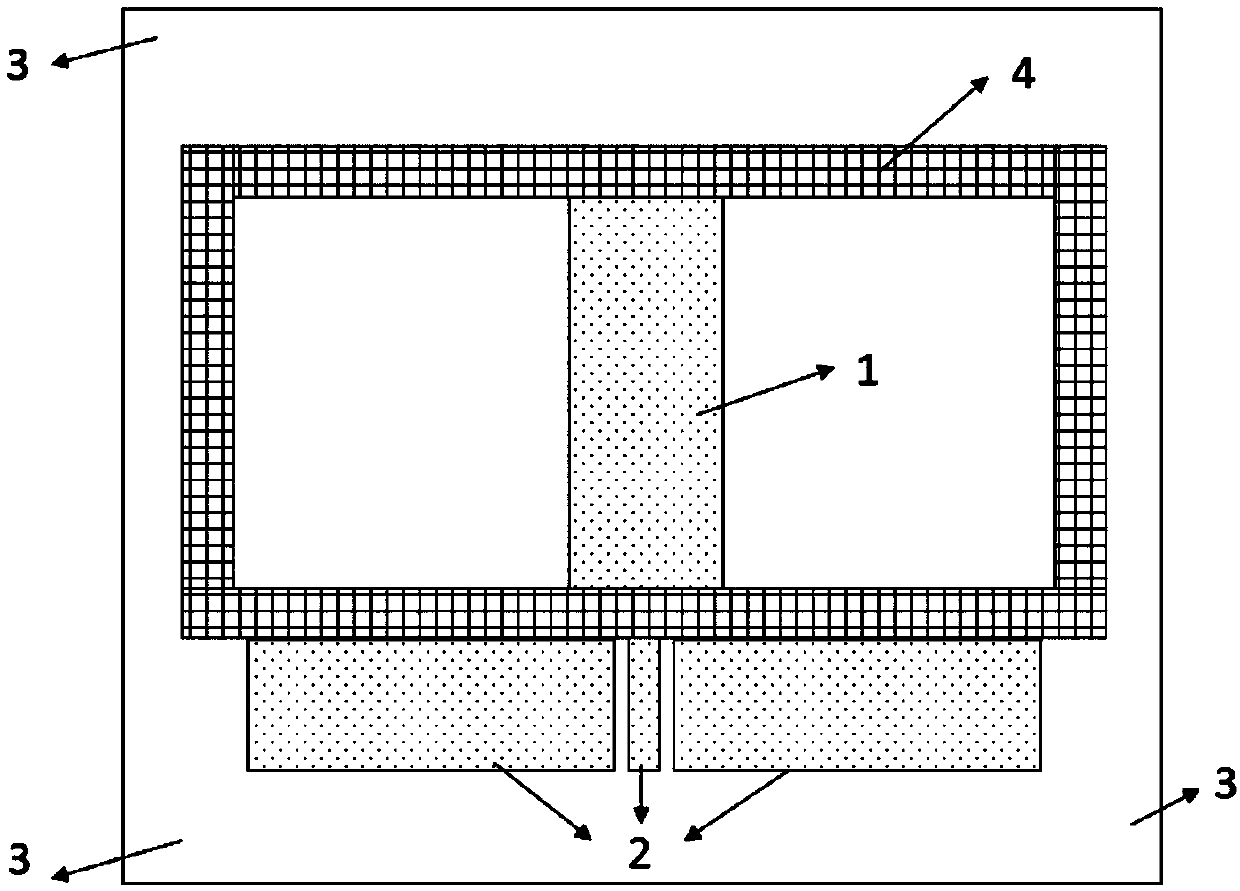
[0050] Such as figure 1 and 4 As shown, a method of making a glucose biosensor based on a microwave patch resonator with a wall structure on the front is as follows:
[0051] (1) First use glass, quartz, silicon and other semiconductor substrates, and use isopropylamine solution to clean once, and then use deionized water to clean twice to ensure that the surface is clean and free of impurities;
[0052] (2) Deposit a layer of silicon dioxide or silicon nitride passivation layer with a thickness of 50-200 nanometers on the semiconductor substrate by using the low-pressure chemical vapor deposition method, so as to obtain a flatter surface for subsequent processing;
[0053] (3) Use the sputtering method to grow a layer of titanium or chromium with a thickness of about 20-50 nanometers as the first seed metal layer, and then use the sputtering method to grow a layer of gold with a thickness of about 30-100 nanometers as the second layer A seed metal layer to promote adhesion ...
Embodiment 2
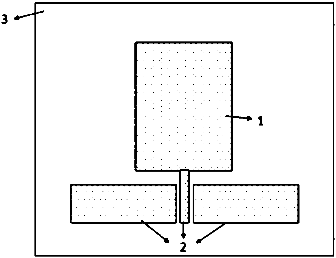
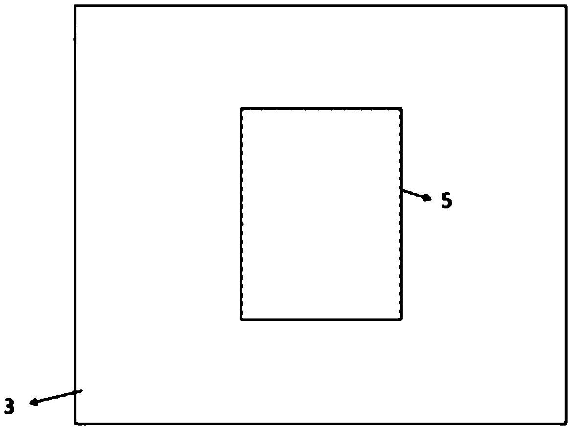
[0065] Such as Figure 2-3 , as shown in 5-6, a glucose biosensor based on a microwave patch resonator with a groove structure on the back is fabricated as follows:
[0066] (1) First use glass, quartz, silicon and other semiconductor substrates, and use isopropylamine solution to clean once, and then use deionized water to clean twice to ensure that the surface is clean and free of impurities;
[0067] (2) Deposit a layer of silicon dioxide or silicon nitride passivation layer with a thickness of 50-200 nanometers on the semiconductor substrate by using the low-pressure chemical vapor deposition method, so as to obtain a flatter surface for subsequent processing;
[0068] (3) Use the sputtering method to grow a layer of titanium or chromium with a thickness of about 20-50 nanometers as the first seed metal layer, and then use the sputtering method to grow a layer of gold with a thickness of about 30-100 nanometers as the second layer A seed metal layer to promote adhesion be...
Embodiment 3
[0087] Detection of glucose solution concentration
[0088](1) Using HFSS v16 software on the computer, two kinds of chip resonators with strict specifications based on the "wall" structure on the front of the substrate and the "groove" structure on the back of the substrate were designed and simulated. figure 1 and figure 2 They are patch resonators based on the front SU-8 "wall" structure and the back "groove" structure;
[0089] (2) The frequency response of the patch resonator should have a high quality factor, and the size of the patch resonator should be slightly smaller than the "wall" and "groove" structures, so as to ensure that the test solution drips into the "wall" and "groove" "The structure can completely cover the patch sensor, touch and affect the electric field of the patch resonator, and finally change the frequency and reflection coefficient of the patch resonator to characterize the concentration of glucose;
[0090] (3) Using micro-nano technology to co...
PUM
| Property | Measurement | Unit |
|---|---|---|
| thickness | aaaaa | aaaaa |
| thickness | aaaaa | aaaaa |
| thickness | aaaaa | aaaaa |
Abstract
Description
Claims
Application Information


