Supercharge Your Innovation With Domain-Expert AI Agents!

Manufacturing method of electromagnetic wave shielding film for flexible printed circuit board

A manufacturing method and shielding film technology, applied in the fields of magnetic field/electric field shielding, chemical instruments and methods, applications, etc., can solve the problems of raw material loss, product yield and physical property decline, and achieve increased productivity, shortened manufacturing processes, and improved economics. sexual effect

Active Publication Date: 2019-06-28
DOOSAN CORP
View PDF7 Cites 0 Cited by
  • Summary
  • Abstract
  • Description
  • Claims
  • Application Information

AI Technical Summary

Problems solved by technology

Thus, when the second multi-layer coating is performed, the loss of raw materials after the first coating inevitably occurs, resulting in a problem that the yield and physical properties of the final product decrease

Method used


Image

  • Manufacturing method of electromagnetic wave shielding film for flexible printed circuit board
  • Manufacturing method of electromagnetic wave shielding film for flexible printed circuit board
  • Manufacturing method of electromagnetic wave shielding film for flexible printed circuit board

Examples


Embodiment 1

[0123] 1-1. Production of insulating layer coating liquid

[0124] The following substances were mixed and dissolved to prepare an insulating layer coating liquid: 9.1% by weight of a halogen-free non-flexible epoxy resin (Kukusu Chemical KDP555) as a thermosetting resin, 8.1% by weight of a bisphenol A type epoxy resin (Dow DER 383), low Dielectric epoxy resin (Nippon XD1000) 3.5% by weight, bisphenol novolac epoxy resin (KPBN110) 6.1% by weight, carbon black (Columbia (Columbian) chemical) 0.9% by weight, phosphorus flame retardant (Otsuka Chemical SPB-100) 4.8% by weight, thermoplastic resin rubber (Kumho Petrochemical KNB 40H) 24.2% by weight, polyvinyl butyral resin (UNO Chemical KS23Z) 12.1% by weight, dicyandiamide as a latent curing agent 10.7% by weight, 0.6% by weight of an imidazole derivative (Ildong Chemical 2E4MZ) as a catalyst-type curing agent, and 9.8% by weight of methyl cellosolve as a solvent.

[0125] 1-2. Preparation of conductive adhesive layer coat...

Embodiment 2-4

[0134] The electromagnetic wave shielding film for flexible printed circuit boards was manufactured by the method similar to the said Example 1 except having changed the thickness of the electrolytic copper foil of the separation-type double-layer copper foil as shown in following Table 1.

[0135] At this time, in Examples 2 to 3, 2 μm electrolytic copper foil (Mitsui (Japan), 2 μm electrolytic copper foil) and 3 μm electrolytic copper foil (Mitsui (Japan), 3 μm electrolytic copper foil) composed of separate double layers were used, respectively. ), and 6 μm rolled copper foil (Mitsui (Japan), 6 μm electrolytic copper foil) composed of a copper single layer was used in Example 4, respectively.

Embodiment 5

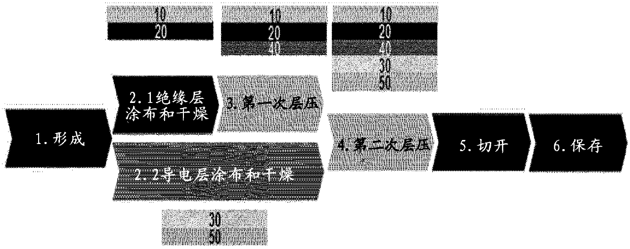
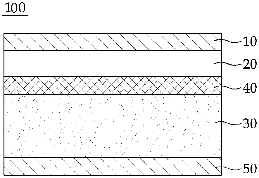
[0137] An insulating layer was formed on the first surface of the first substrate film by microgravure coating using the insulating layer coating composition produced in Example 1-1, and dried at 130° C. for 3 minutes and 30 seconds, An insulating layer of 5 to 6 μm in a semi-cured state was formed.

[0138] By comma coating, using the conductive adhesive layer composition produced in Example 1-2, a conductive adhesive layer was formed on the first surface of the second base film prepared later, and dried at 130° C. for 3 In minutes and 30 seconds, a semi-cured conductive layer of 14 to 15 μm was formed.

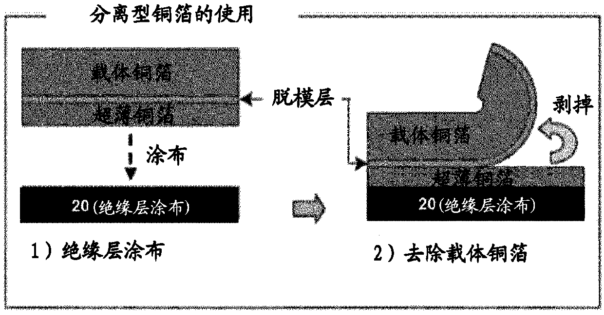
[0139] Use separation-type (Peelable) double-layer copper foil [electrolytic copper foil (1μm) + separation layer + carrier copper foil (35μm), Olin Brass (USA), 1μm electrolytic copper foil), on the first substrate film After bonding the second copper foil of the split-type double-layer copper foil to the insulating layer, the first copper foil of the carrier was removed. ...


PUM

PropertyMeasurementUnit
thicknessaaaaaaaaaa
thicknessaaaaaaaaaa
thicknessaaaaaaaaaa

Abstract

The present invention provides a method for manufacturing an electromagnetic wave shielding film, comprising: (i) coating a thermosetting resin composition for forming an insulating layer on a first surface of a first substrate film to form an insulating layer; (ii) A peelable double-layer copper foil composed of a second copper foil, an adhesive layer, and a carrier first copper foil is laminated on the insulating layer, and the carrier first copper foil is removed after bonding the insulating layer and the second copper foil (iii) coating a conductive adhesive layer-forming resin composition comprising a conductive filler and a thermosetting resin on the first surface of the second base film and drying to form a conductive adhesive layer; and (iv) laminating the first base film and the second base film, and disposing the second copper foil of the first base film and the conductive adhesive layer of the second base film in contact with each other and then pressurizing Steps in the process of crimping. In the present invention, not only can the loss of raw materials caused by repeated multi-layer coating processes to form multiple coating layers in the conventional production of electromagnetic wave shielding films be minimized, but also the production process can be simplified to improve economical efficiency.

Description

technical field [0001] The present invention relates to a new manufacturing method of a shielding film for shielding electromagnetic waves generated in electronic components such as printed circuit boards used in electronic products such as computers, communication equipment, printers, mobile phones, and video cameras, and communication equipment such as cables and wires, or communication components. Background technique [0002] In general, demands for miniaturization, planarization, and high functionality of electronic devices are gradually increasing. In order to meet these requirements, components with different use frequency domains are used in the same electronic equipment, resulting in complex electromagnetic wave noise, which increases the difficulty of taking measures against this complex electromagnetic wave noise. At the same time, there is an increasing demand for thinner data transmission cables and less emission of electromagnetic wave noise. When transmitting...

Claims


Application Information

Patent Timeline
Patent Type & Authority Patents(China)
IPC IPC(8): B32B15/08B32B15/20B32B27/00B32B37/10B32B37/12B32B37/26B32B33/00H05K9/00
CPCB32B15/08B32B15/20B32B27/00B32B33/00B32B37/10B32B37/1284B32B37/26B32B2037/268B32B2255/10B32B2255/26B32B2307/212B32B2311/12B32B2457/08H05K9/0088B32B37/12H05K9/00
Inventor 朴汉性曺景橒金宇贞柳正燮
Owner DOOSAN CORP
Features
  • R&D
  • Intellectual Property
  • Life Sciences
  • Materials
  • Tech Scout
  • Unparalleled Data Quality
  • Higher Quality Content
  • 60% Fewer Hallucinations
Learn More