Pixel unit circuit, driving method, pixel circuit, and display device

A technology of a pixel unit and a driving method, which is applied in the fields of pixel unit circuits, pixel circuits and display devices, can solve the problems of unstable luminous brightness of light-emitting elements, inability to stably maintain, and inability to increase the size of storage capacitors, etc.

Inactive Publication Date: 2017-12-01
BOE TECH GRP CO LTD
View PDF6 Cites 13 Cited by
  • Summary
  • Abstract
  • Description
  • Claims
  • Application Information

AI Technical Summary

Problems solved by technology

[0003] The main purpose of the present invention is to provide a pixel unit circuit, a driving method, a pixel circuit and a display device, so as to solve the problem that the driving transistor for driving silicon-based OLED (organic light-emitting diode) to emit light in the prior art works in the sub-threshold region, which leads to the need to The size of the driving transistor is set too large, so it cannot be applied to high-resolution display products, and the size of the storage capacitor cannot be made large, which leads to the problem that the luminance of the light-emitting element cannot be stabilized due to the inability to maintain the data voltage stably.

Method used


Image

  • Pixel unit circuit, driving method, pixel circuit, and display device
  • Pixel unit circuit, driving method, pixel circuit, and display device
  • Pixel unit circuit, driving method, pixel circuit, and display device

Examples


Embodiment Construction

[0045] The following will clearly and completely describe the technical solutions in the embodiments of the present invention with reference to the accompanying drawings in the embodiments of the present invention. Obviously, the described embodiments are only some, not all, embodiments of the present invention. Based on the embodiments of the present invention, all other embodiments obtained by persons of ordinary skill in the art without making creative efforts belong to the protection scope of the present invention.

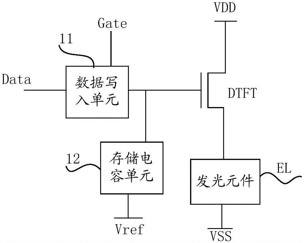
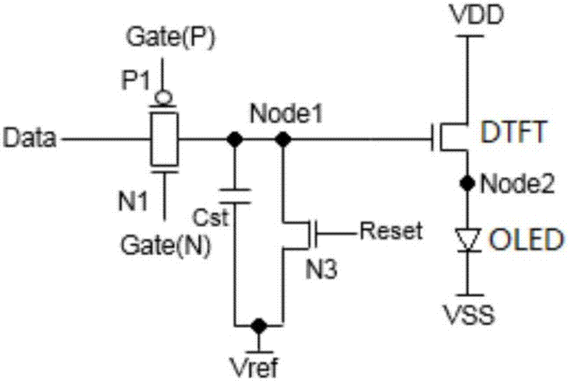
[0046]The transistors used in all the embodiments of the present invention can be thin film transistors or field effect transistors or other devices with the same characteristics. In the embodiment of the present invention, in order to distinguish the two poles of the transistor except the gate, one pole is called the first pole, and the other pole is called the second pole. In actual operation, the first electrode may be a drain, and the second electrode may ...


PUM


Abstract

The invention provides a pixel unit circuit, a driving method, a pixel circuit, and a display device. The pixel unit circuit comprises a light-emitting component, a drive transistor, a data writing-in unit, and a storage capacitance unit. The data writing-in unit is connected with a data line, a grid line, and a grid electrode of the drive transistor, and is used to control to connect or disconnect connection between the data line and the grid electrode of the drive transistor under control of the grid line. A first end of the storage capacitance unit is connected with the grid electrode of the drive transistor. A second end of the storage capacitance unit is connected with a reference voltage input end. A second end of the light-emitting component is connected with a low-level input end. Through changing potential of the grid electrode of the drive transistor, voltage of a source electrode of the drive transistor is changed, and through adjusting voltage difference between a first end of the light-emitting component and a second end of the light-emitting component, luminance of the light-emitting component is adjusted.

Description

technical field [0001] The present invention relates to the field of display technology, in particular to a pixel unit circuit, a driving method, a pixel circuit and a display device. Background technique [0002] The luminance of silicon-based OLED (Organic Light-Emitting Diode, Organic Light-Emitting Diode) is usually controlled by driving the current in the subthreshold region of MOS tube (metal-oxide-semiconductor field-effect transistor) , since the current of the MOS tube is proportional to its width-to-length ratio, in order to realize the small current of the micro-display pixel, the ratio of W / L (width-to-length ratio) must be designed very small, that is, the length L of the driving MOS tube must be designed It is very large; in this way, it is difficult to apply to high-resolution products, the storage capacitor cannot be enlarged, and the data voltage cannot be maintained stably, resulting in unstable OLED brightness. Moreover, the subthreshold current of the MO...

Claims


Application Information

Patent Timeline
IPC IPC(8): G09G3/3258
CPCG09G3/3258G09G2320/0626G09G3/3233G09G2300/0842G09G2310/0251G09G2320/0233G09G3/3241G09G3/3291
Inventor 玄明花陈小川杨盛际
Owner BOE TECH GRP CO LTD
Why Eureka
Try Eureka