Optimum design method applied to industrial camera circuit board

An optimized design and industrial camera technology, applied to color TV parts, TV system parts, TV, etc., can solve the problems of high production cost, poor utilization rate, large size, etc., and achieve weight reduction, size reduction, The effect of reducing production costs

Inactive Publication Date: 2017-12-08
CHANGCHUN INST OF OPTICS FINE MECHANICS & PHYSICS CHINESE ACAD OF SCI
View PDF5 Cites 2 Cited by
  • Summary
  • Abstract
  • Description
  • Claims
  • Application Information

AI Technical Summary

Problems solved by technology

[0004] In order to solve the problems that the existing industrial camera is realized by two circuit boards, there are problems such as large size, high production cost and poor utilization rate, the present invention provides an optimized design method applied to the industrial camera circuit board

Method used


Image

  • Optimum design method applied to industrial camera circuit board
  • Optimum design method applied to industrial camera circuit board

Examples


specific Embodiment approach 1

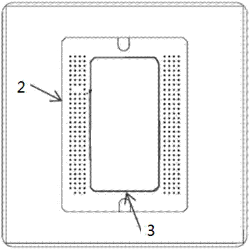
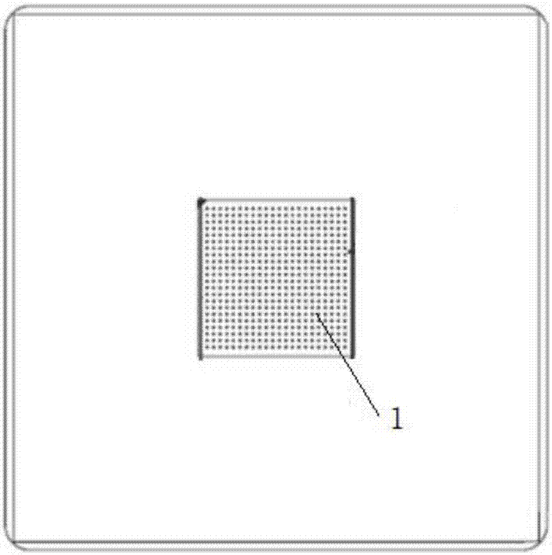
[0013] Specific implementation mode one, combination figure 1 with figure 2 The description of this embodiment is applied to the optimized design method of industrial camera circuit board, including image sensor and FPGA control chip. The FPGA control chip and the image sensor socket 2 are respectively laid out at the center of the front and the center of the back of the same circuit board. The image sensor socket 2 is packaged by BGA and has a leakage area 3 in the middle; the image sensor is inserted in the image On the sensor socket 2, the image sensor and the FPGA control chip are directly connected through a circuit board; the filter capacitor 1 of the FPGA control chip is arranged in the leakage area 3 of the image sensor socket.

[0014] In this embodiment, the FPGA control chip selects the smallest package model that meets the functional requirements, and the FPGAG control chip model selects the smallest package model as the XC6SLX100CSG484 model. A large number of filt...


PUM


Abstract

The invention discloses an optimum design method applied to an industrial camera circuit board, relates to the field of an industrial camera circuit system and solves the problem that an existing industrial camera is realized by two circuit boards, so the existing industrial camera is large in size, high in production cost and low in utilization rate. An FPGA control chip and an image sensor socket are laid out at the front central position and the back central position of the same circuit board. The image sensor socket is a structure packaged through BAG. The middle of the image sensor socket is hollowed. An image sensor is plugged into the image sensor socket. The image sensor and the FPGA control chip are directly connected through the circuit board. A filter capacitor of the FPGA control chip is laid out at the hollowed position of the image sensor socket. The image sensor and the FPGA control chip are optimally designed on one circuit board, so the size of one circuit board is reduced, and moreover, an area occupied by a connector is removed. According to the method provided by the invention, the features such as a small size, the light weight, the low cost, the high reliability and a replicable sensor of the industrial camera are satisfied.

Description

Technical field [0001] The invention relates to the field of industrial camera circuit system design, in particular to an optimized design method applied to industrial camera circuit boards. Background technique [0002] An industrial camera is a key component in a machine vision system. Its most essential function is to convert light signals into orderly electrical signals. Choosing the right camera is an important part of the machine vision system design. The choice of camera not only directly determines the collection The resulting image resolution and image quality are also directly related to the operating mode of the entire system. [0003] With the rapid development of the electronics industry, industrial cameras based on different image sensors have been widely developed and applied. The imaging quality, stability, reliability, weight, volume and price of industrial cameras have become the key to their development prospects. Industrial cameras are also developing in the di...

Claims


Application Information

Patent Timeline
IPC IPC(8): H04N5/225H04N5/247
CPCH04N23/50H04N23/90
Inventor 冯汝鹏徐伟朴永杰章家保金光周美丽
Owner CHANGCHUN INST OF OPTICS FINE MECHANICS & PHYSICS CHINESE ACAD OF SCI
Why Eureka
Try Eureka