Array substrate, display panel and display device
An array substrate and display area technology, which is applied in the direction of instruments, electrical digital data processing, and data processing input/output process, and can solve the problems of pressure sensing signal lines occupying non-display areas and widening of the border of array substrates, etc.
- Summary
- Abstract
- Description
- Claims
- Application Information
AI Technical Summary
Problems solved by technology
Method used
Image
Examples
Embodiment Construction
[0029] The present invention will be further described in detail below in conjunction with the accompanying drawings and embodiments. It should be understood that the specific embodiments described here are only used to explain the present invention, but not to limit the present invention. In addition, it should be noted that, for the convenience of description, only some structures related to the present invention are shown in the drawings but not all structures.
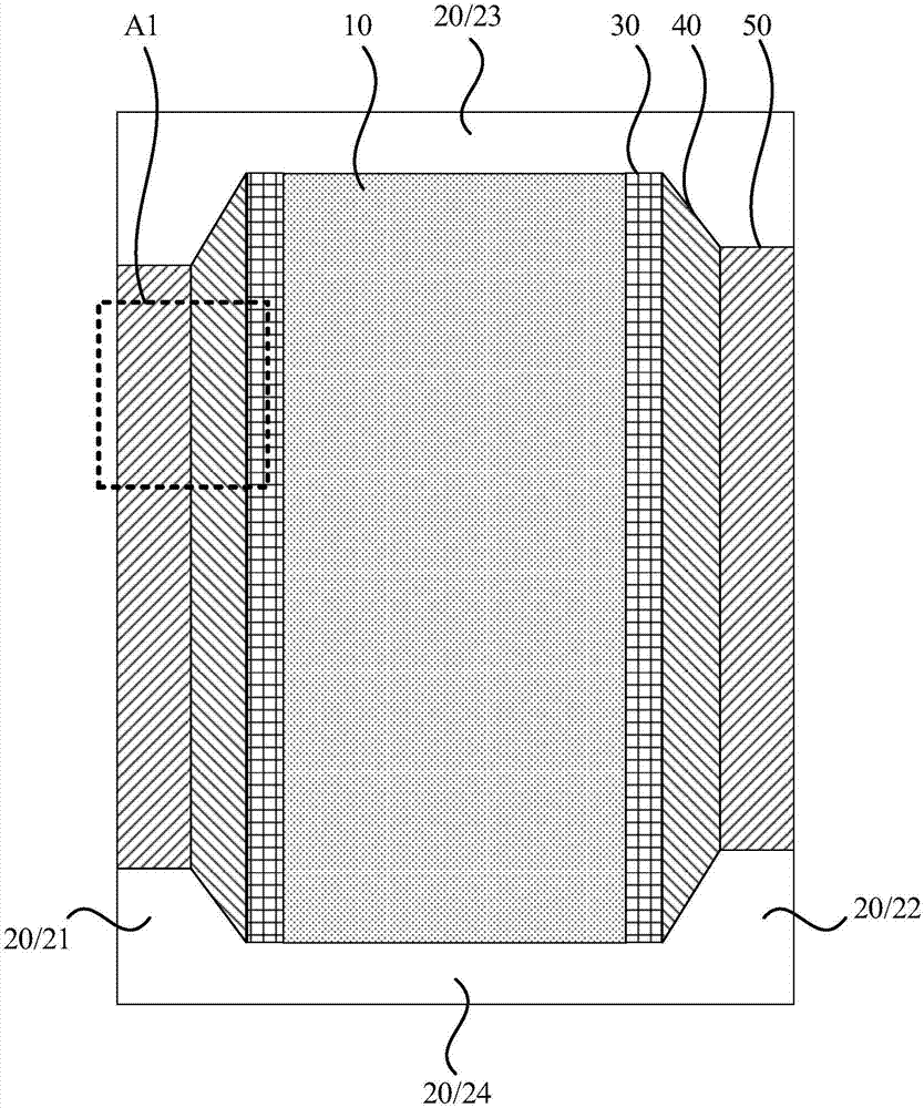
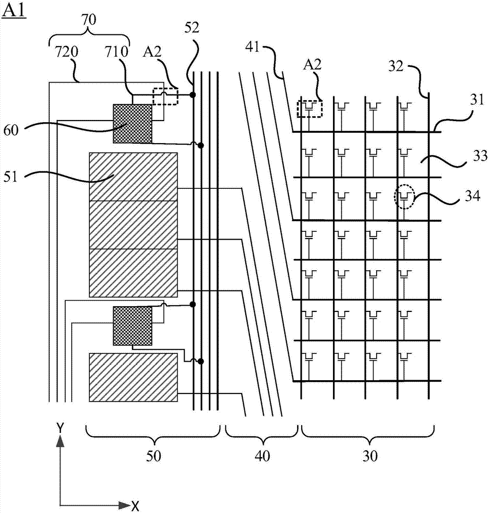
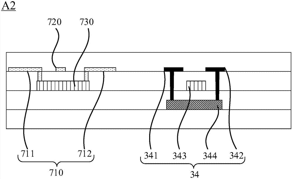
[0030] figure 1 It is a schematic top view structure diagram of an array substrate provided by an embodiment of the present invention, figure 2 for figure 1 A schematic diagram of an enlarged structure of the A1 region in the middle, combined with figure 1 and figure 2 As shown, the array substrate includes a display area 10 and a non-display area 20 located on the periphery of the display area. The non-display area 20 includes a first non-display area 21, a second non-display area 22, a third non-display are...
PUM
 Abstract
Description
Claims
Application Information


