Shift register, driving method thereof, driving control circuit and display device
A shift register and control electrode technology, applied in static memory, digital memory information, instruments, etc., can solve the problems of increased process difficulty, increased production cost, complicated connection structure, etc., so as to reduce production cost and simplify preparation. Craftsmanship to achieve the effect of narrow bezel design
- Summary
- Abstract
- Description
- Claims
- Application Information
AI Technical Summary
Problems solved by technology
Method used
Image


Examples
Embodiment 1
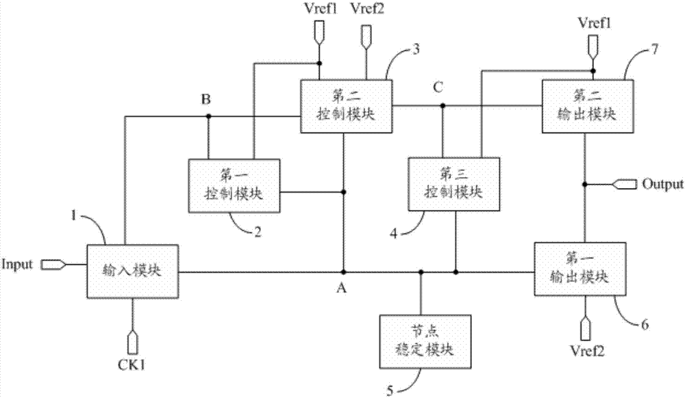
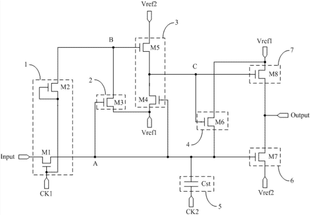
[0107] by Figure 2a The structure of the shift register shown is taken as an example to describe its working process; the signal of the first reference signal terminal Vref1 is a high potential signal, and the signal of the second reference signal terminal Vref2 is a low potential signal; the corresponding input and output timing diagram Such as Figure 3a Shown, specifically, select as Figure 3a The four stages of T1, T2, T3 and T4 in the shown input and output timing diagram.
[0108] In the T1 stage, Input=1, CK1=0, CK2=1.
[0109] Since CK1=0, both the first switch transistor M1 and the second switch transistor M2 are turned on. Among them, the turned-on first switch transistor M1 provides the high-potential signal of the input signal terminal Input to the first node A, so that the signal of the first node A is a high-potential signal, so the third switch transistor M3 and the fourth switch transistor M4 And the seventh switching transistor M7 is turned off. The tur...
Embodiment 2
[0124] by Figure 2a The structure of the shift register shown is described as an example to describe its specific working process. An insertion stage T01 is inserted between the T1 stage and the T2 stage in the timing diagram of the first embodiment, that is, on the basis of the first embodiment, the input The duration of the effective pulse signal at the signal terminal Input is extended by one clock cycle, and the corresponding input and output timing diagram is as follows Figure 3b shown. exist Figure 3b In the timing diagram shown, five stages T1, T01, T2, T3, and T4 are selected, wherein the inserting stage T01 is further divided into a first inserting sub-stage T011 and a second inserting sub-stage T012.
[0125] In the T1 stage, Input=1, CK1=0, CK2=1; and thereafter, Input=1, CK1=1, CK2=1. The specific working process of this stage is basically the same as that of the T1 stage in Embodiment 1, and will not be described in detail here.
[0126] In the T011 phase o...
Embodiment 3
[0139] by Figure 2a The structure of the shift register shown is taken as an example to describe its specific working process. Two insertion stages T01 and T02 are inserted between the T1 stage and the T2 stage in the timing diagram of the first embodiment, that is, on the basis of the first embodiment The duration of the effective pulse signal at the input signal terminal Input is extended by two clock cycles, and the corresponding input and output timing diagram is as follows Figure 3c shown. exist Figure 3c In the timing diagram shown, six stages T1, T01, T02, T2, T3, and T4 are selected, among which, the insertion stage T01 is further divided into the first insertion sub-stage T011 and the second insertion sub-stage T012; the insertion stage T02 is further divided into It is the first insertion sub-phase T021 and the second insertion sub-phase T022.
[0140] In the T1 stage, Input=1, CK1=0, CK2=1; and thereafter, Input=1, CK1=1, CK2=1. The specific working process o...
PUM
 Abstract
Description
Claims
Application Information
 - R&D
- Intellectual Property
- Life Sciences
- Materials
- Tech Scout
- Unparalleled Data Quality
- Higher Quality Content
- 60% Fewer Hallucinations
Browse by: Latest US Patents, China's latest patents, Technical Efficacy Thesaurus, Application Domain, Technology Topic, Popular Technical Reports.
© 2025 PatSnap. All rights reserved.Legal|Privacy policy|Modern Slavery Act Transparency Statement|Sitemap|About US| Contact US: help@patsnap.com