Method and reagent for increasing yield of selectively dispersed semiconducting carbon nanotubes

A semiconducting and carbon nanotube technology, which is applied in the field of improving the yield of selectively dispersed semiconducting single-wall carbon nanotubes and the separation of semiconducting single-wall carbon nanotubes, can solve the problem of high semiconductor purity, low purity and low yield. and other problems, to achieve the effect of improving repeatability and stability, wide source of raw materials, and reducing costs

Active Publication Date: 2020-05-19
SUZHOU INST OF NANO TECH & NANO BIONICS CHINESE ACEDEMY OF SCI
View PDF4 Cites 0 Cited by
  • Summary
  • Abstract
  • Description
  • Claims
  • Application Information

AI Technical Summary

Problems solved by technology

Among them, selective dispersion has been developed rapidly due to its simple operation, ultra-high semiconductor purity and low loss to single-walled carbon tubes, but low yield is one of the bottlenecks of this method.
[0005] At present, there is still a method to selectively disperse and separate single-walled carbon nanotubes by using a single polythiophene or a single polycarbazole, but the semiconducting single-walled carbon nanotubes obtained by using a single polythiophene method have high yields but low purity. ; and the semiconducting single-walled carbon nanotubes obtained by the method of single polycarbazole, although the purity is high, the yield is low

Method used


Image

  • Method and reagent for increasing yield of selectively dispersed semiconducting carbon nanotubes
  • Method and reagent for increasing yield of selectively dispersed semiconducting carbon nanotubes
  • Method and reagent for increasing yield of selectively dispersed semiconducting carbon nanotubes

Examples


Embodiment 1

[0045] In this embodiment, polycarbazole (PCO) and polythiophene (rr-P3DDT) are selected as the dual polymer system, and their structural formulas are respectively:

[0046]

[0047] (1) Mix polycarbazole, polythiophene, and single-walled carbon nanotube samples in a ratio of 2:2:1, and then add a certain amount of toluene to the formed mixture so that the concentration of polycarbazole and polythiophene is 0.5 mg / ml;

[0048] (2) Place the above mixed solution in a probe sonicator for sonication, keep the temperature at 20° C., power at 3-10 W / ml, and time for 0.5-2 hours. After the ultrasound is over, use a centrifuge to centrifuge at a centrifugal force of 20,000-100,000g for 0.5-2 hours, and finally take out 80% of the supernatant to obtain a semiconducting single-walled carbon nanotube solution with a purity greater than 99% and a concentration greater than 50ug / ml .

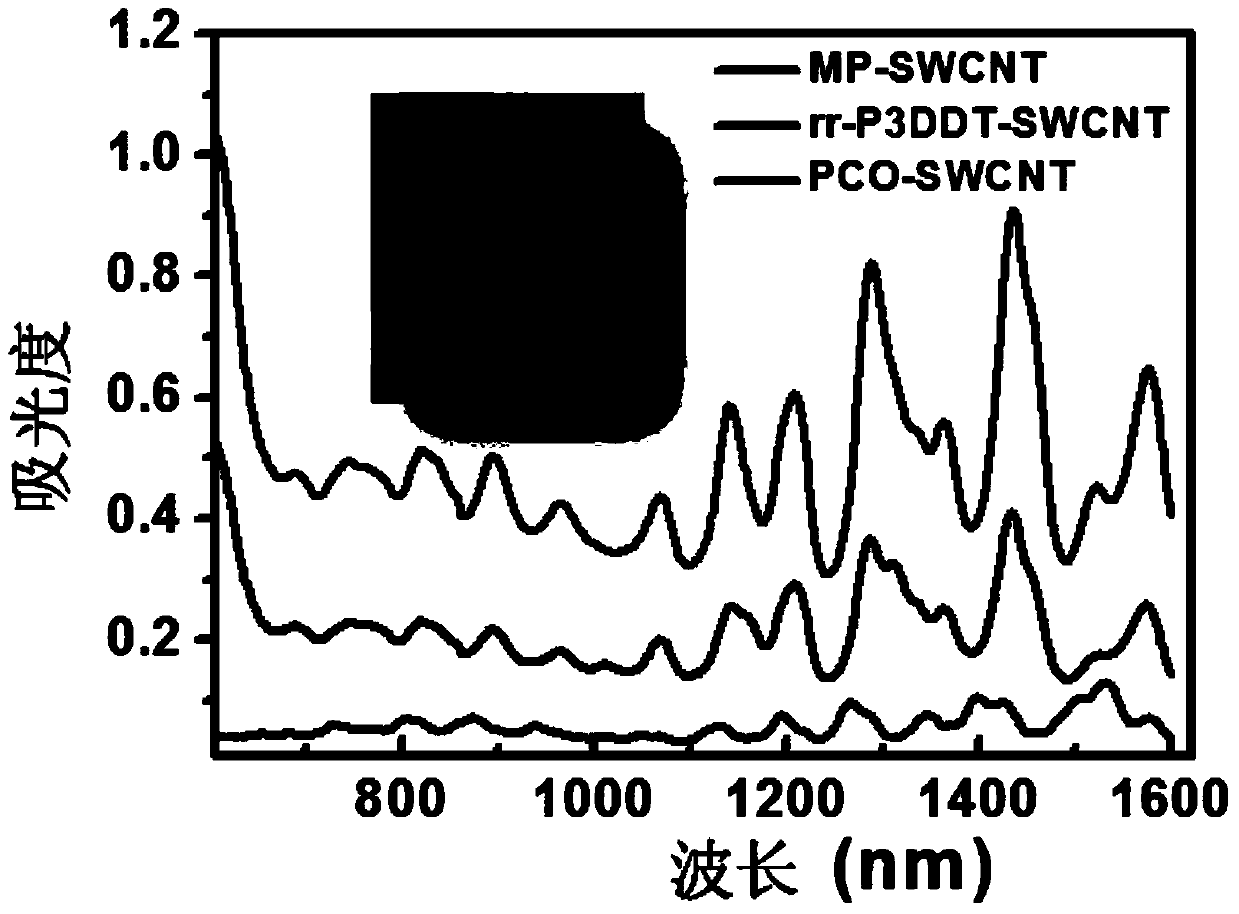
[0049] figure 1 Absorption spectra of PCO, rr-P3DDT and PCO / rr-P3DD mixture dispersed and separate...

Embodiment 2

[0051] (1) Mix polyfluorene, polythiophene, and single-walled carbon nanotube samples in a ratio of 2:2:1, and then add a certain amount of toluene to the formed mixture so that the concentration of polycarbazole and polythiophene is 0.5mg / ml;

[0052] (2) Place the above mixed solution in a probe sonicator for sonication, keep the temperature at 20° C., power at 3-10 W / ml, and time for 0.5-2 hours. After the ultrasound is over, use a centrifuge to centrifuge at a centrifugal force of 20,000-100,000g for 0.5-2 hours, and finally take out 80% of the supernatant to obtain a semiconducting single-walled carbon nanotube solution with a purity greater than 99% and a concentration greater than 50ug / ml .

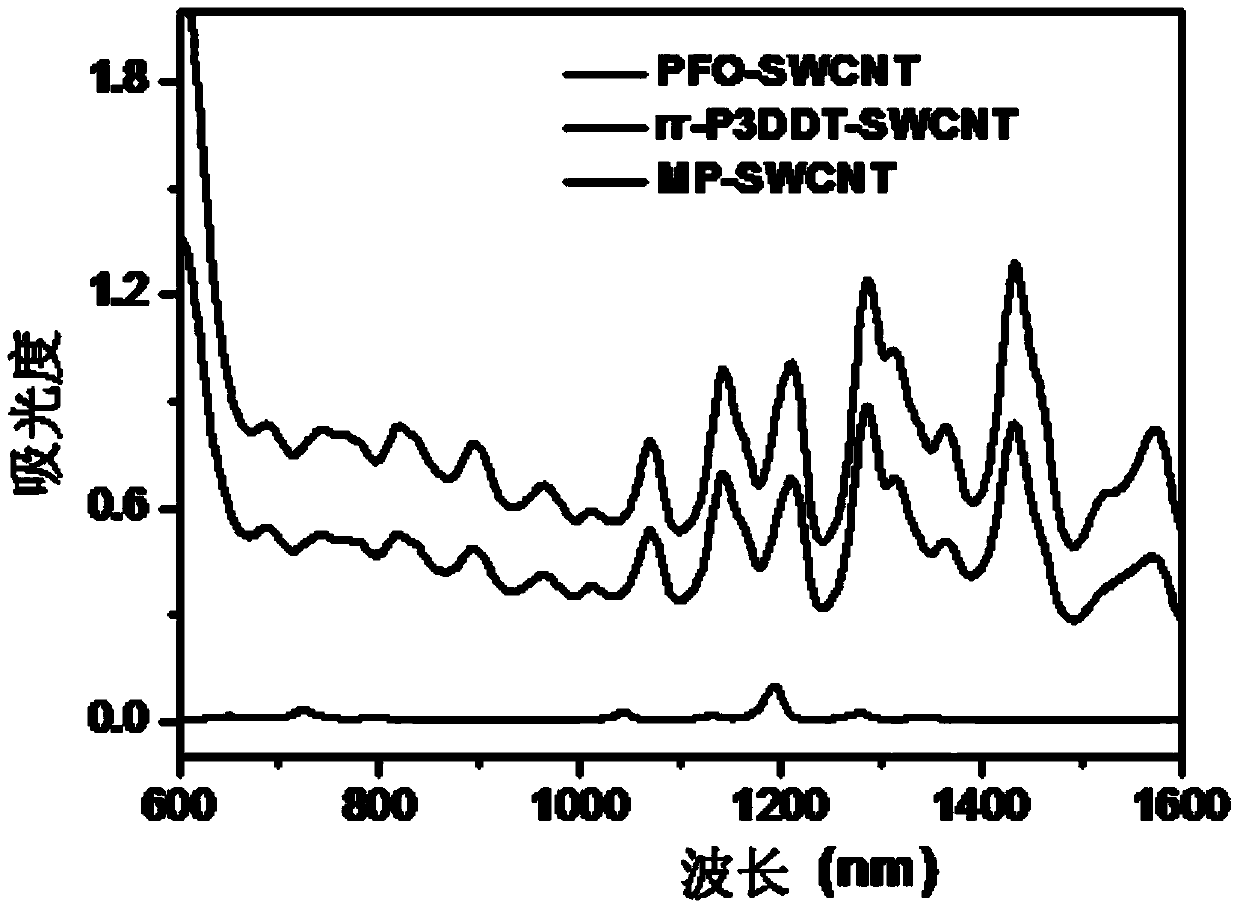
[0053] image 3 The absorption spectra of PFO, rr-P3DDT and PFO / rr-P3DD mixture dispersed and separated single-walled carbon nanotubes, respectively.

[0054] In addition, the inventor of this case also referred to the scheme of the aforementioned Examples 1-2, and carried out ...


PUM

PropertyMeasurementUnit
concentrationaaaaaaaaaa
purityaaaaaaaaaa

Abstract

The invention discloses a method and a reagent for increasing the yield of selectively dispersed semiconducting carbon nanotubes. The method comprises: uniformly mixing the single-wall carbon nanotube sample, the first polymer and the second polymer in a solvent to form a liquid phase mixing system, and fully dispersing the single-wall carbon nanotube sample in the liquid phase mixing system, Afterwards, the liquid-phase mixed system is centrifuged to separate the supernatant to realize the selective separation of semiconducting single-walled carbon nanotubes; both the first polymer and the second polymer can specifically bind to semiconducting single-walled carbon nanotubes, And the binding speed of the first polymer and the semiconducting single-walled carbon nanotube is greater than the binding speed of the second polymer and the semiconducting single-walled carbon nanotube, and the binding strength is lower than that of the second polymer and the semiconducting single-walled carbon nanotube Bond strength. The invention can realize selective separation of semiconducting single-wall carbon nanotubes with high yield, high purity and high dispersibility, reduces cost, and improves separation repeatability and stability.

Description

technical field [0001] The invention relates to a method for separating semiconducting single-walled carbon nanotubes, in particular to a method for increasing the yield of selectively dispersed semiconducting single-walled carbon nanotubes, which belongs to the technical field of carbon nanotubes. Background technique [0002] Carbon Nanotubes (CNTs for short) is a new type of carbon structure discovered in 1991. It is a tube formed by graphene sheets formed by carbon atoms. Carbon nanotubes have small diameters and large aspect ratios, and are considered quasi-one-dimensional nanomaterials. Because carbon nanotubes have excellent electrical properties and super mechanical properties, they have attracted great attention in the field of materials. [0003] Due to their excellent electrical properties, single-walled carbon nanotubes (SWCNTs) have broad application prospects in the field of electronics, and are important candidates for the next generation of semiconductor mat...

Claims


Application Information

Patent Timeline
Patent Type & Authority Patents(China)
IPC IPC(8): C01B32/172C01B32/159
CPCC01P2002/82C01P2002/84C01P2006/80C01B32/174C01B2202/02C01B2202/22C01B32/158C01B32/159C01B32/172C01P2006/40
Inventor 李清文刘丹邱松张锦金赫华李红波
Owner SUZHOU INST OF NANO TECH & NANO BIONICS CHINESE ACEDEMY OF SCI
Why Eureka
Try Eureka