Substrate processing device
A substrate processing device and substrate technology, which is applied in the direction of electrical components, semiconductor/solid-state device manufacturing, circuits, etc., can solve the problems of narrowing the range of material selection and inability to form holding parts, etc.
- Summary
- Abstract
- Description
- Claims
- Application Information
AI Technical Summary
Problems solved by technology
Method used
Image

Examples
Embodiment approach
[0127] The present invention is not limited to the contents of the above-described embodiments, and various changes can be made within the scope of the present invention.
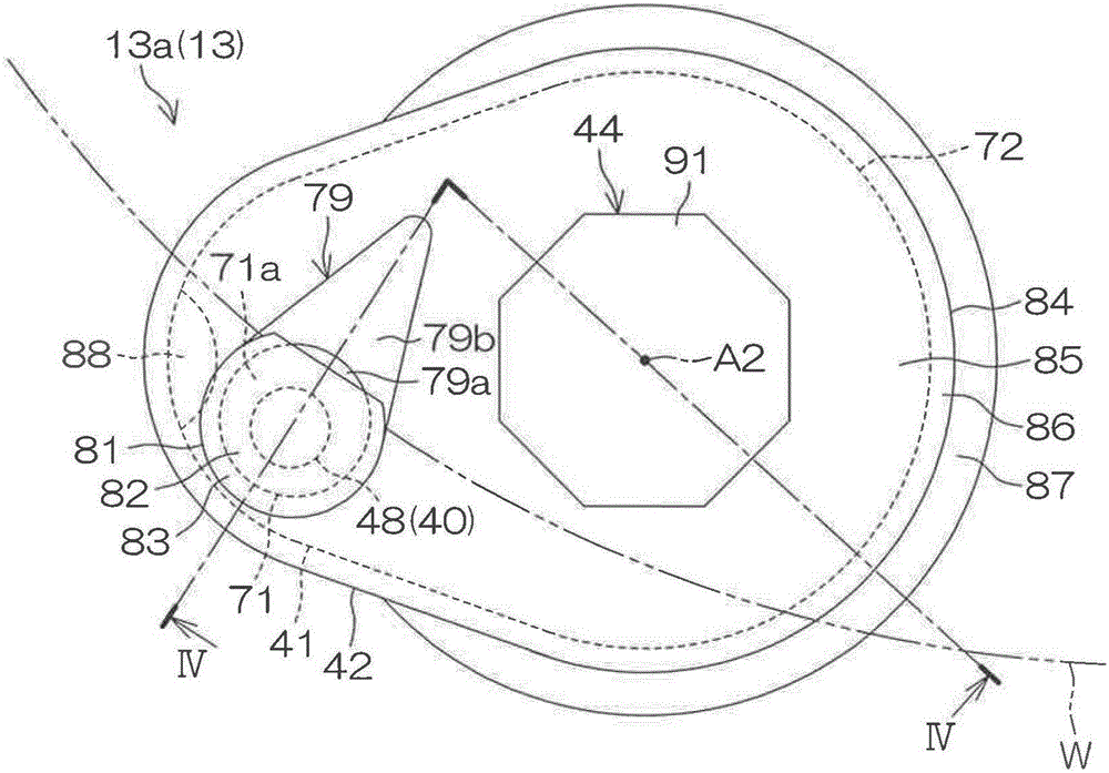
[0128] For example, in the above-mentioned embodiment, the case where the jig cover 42 covers the entire exposed portion of the conductive member 41 in a plan view has been described, but the jig cover 42 may cover only a part of the exposed portion in a plan view. The jig cover 42 may also be omitted.
[0129] The softening temperature of the entire core material 40 may be the same as or lower than the softening temperature of the entire conductive member 41 . Likewise, the strength of the entire core material 40 may be equal to or lower than the strength of the entire conductive member 41 .
[0130] At least one of the upper facing portion (lower surface 91 a ) of the current conducting member 44 and the lower facing portion (hook portion 88 ) of the jig cover 42 may be omitted as long as the jig cover 4...
PUM
 Abstract
Description
Claims
Application Information
 - R&D
- Intellectual Property
- Life Sciences
- Materials
- Tech Scout
- Unparalleled Data Quality
- Higher Quality Content
- 60% Fewer Hallucinations
Browse by: Latest US Patents, China's latest patents, Technical Efficacy Thesaurus, Application Domain, Technology Topic, Popular Technical Reports.
© 2025 PatSnap. All rights reserved.Legal|Privacy policy|Modern Slavery Act Transparency Statement|Sitemap|About US| Contact US: help@patsnap.com