pcb signal unit shielding grounding device
A signal unit, shielding and grounding technology, applied in the field of PCB signal unit shielding and grounding devices, can solve problems such as grounding faults, mutual interference, poor grounding of PCB signal units, etc., achieve good grounding effect, and prevent the effect of mutual interference of electromagnetic signals
- Summary
- Abstract
- Description
- Claims
- Application Information
AI Technical Summary
Problems solved by technology
Method used
Image
Examples
Embodiment
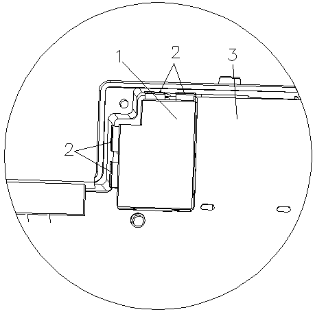
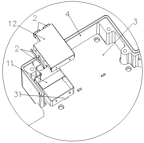
[0046] Such as figure 1 with figure 2 As shown, the shielding and grounding device of the PCB signal unit includes a shielding cover 1 for covering the PCB signal unit, and the outer side of the shielding cover 1 is connected with a connecting piece 2. After the shielding cover 1 is covered and closed on the PCB signal unit, the The connecting piece 2 is in contact with the inner wall of the chassis shell 4 where the PCB board 3 is installed.
[0047] Set the shielding cover 1, cover the PCB signal unit through the shielding cover 1, so as to isolate the PCB signal unit from other signal units, prevent electromagnetic signals from interfering with each other, and achieve a shielding effect. At the same time, set the connecting piece 2 on the shielding cover 1 , when the shielding cover 1 covers the PCB signal unit, the connecting piece 2 contacts the inner wall of the chassis shell 4, so as to realize the grounding of the PCB signal unit, thereby better protecting the signal...
PUM
 Abstract
Description
Claims
Application Information


