Bracket-free packaged LED light source and preparation method thereof

An LED light source, no bracket technology, applied in electrical components, circuits, semiconductor devices, etc., can solve the problems of increased bracket cost, poor sealing, poor glue bonding, etc., to save costs, improve sealing, and reduce machine labor costs Effect

Pending Publication Date: 2018-01-26
SHENZHEN LEPOWER CO LTD
0 Cites 3 Cited by

AI-Extracted Technical Summary

Problems solved by technology

[0002] The general packaging method of the existing LED light source is to use the PCB or the bracket as the carrier. On this basis, the solder spot powder is solidified, and the substrate is indispensable for repackaging. The material of the s...

Abstract

The invention discloses a bracket-free packaged LED light source, which comprises a silver plated copper piece, a first molding adhesive, a wafer and a second molding adhesive, and is characterized inthat the silver plated copper piece is provided with the first molding adhesive thereon and is connected with the first molding adhesive, the wafer is arranged on the first molding adhesive and is connected with the first molding adhesive, the second molding adhesive is packaged on the first molding adhesive, and the wafer is packaged in the second molding adhesive. Another purpose of the invention lies in providing a preparation method of the bracket-free packaged LED light source. The preparation method comprises the steps of S1, preparing materials; S2, manufacturing a silver plated copperpiece; and S3, performing an LED packaging process on the silver plated copper piece. According to the bracket-free packaged LED light source provided by the invention, the molding adhesives are adopted for packaging after the silver plated copper piece is fixed and welded, the sealing performance is improved, and the combination of the silver plated copper piece and the molding adhesives is provided. Meanwhile, the traditional bracket is removed, a bracket-free packaging mode is realized, the machine and labor cost at the upstream and the downstream is greatly reduced, and the cost is saved.

Application Domain

Technology Topic

Image

  • Bracket-free packaged LED light source and preparation method thereof
  • Bracket-free packaged LED light source and preparation method thereof
  • Bracket-free packaged LED light source and preparation method thereof

Examples

  • Experimental program(1)

Example Embodiment

[0065] The present invention will be further described below in conjunction with the drawings and embodiments:
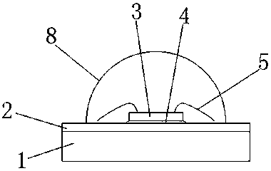
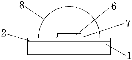
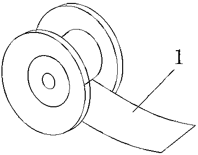
[0066] Such as Figure 1 to Figure 5 As shown, a packaged LED light source without a bracket includes a silver-plated copper sheet 1, a first mold top glue 2, a chip 3, and a second mold top glue 4. The silver-plated copper sheet 1 is provided with a first mold top glue 2 and connected with the first mold top glue 2, the chip is set on the first mold top glue 2 and connected with the first mold top glue 2, the second mold top glue seal 8 is installed on the first mold top glue 2 and The chip is packaged in the second mold top glue 4.
[0067] The beneficial effects of the bracket-free packaged LED light source provided by this embodiment are: the bracket-free packaged LED light source provided by the present invention uses mold top glue to package after the silver-plated copper sheet 1 is solid-soldered, which improves the sealing performance and provides The combination of the silver-plated copper sheet 1 and the mold top glue, and at the same time, the traditional bracket is eliminated, and a bracketless packaging method is realized, which greatly reduces the labor cost of the upstream and downstream machines and saves costs; the first mold top glue 2 Covering the silver-plated copper sheet 1 can protect the silver-plated copper sheet 1 from oxidation.
[0068] In one embodiment, it also includes phosphor, which is coated on the wafer. Coating phosphor powder on the wafer can be made into an LED light source that emits white light.
[0069] In one embodiment, the wafer is a formal wafer 3.
[0070] In one embodiment, a bonding glue 4 is provided between the silver-plated copper sheet 1 and the formal chip 3, and the silver-plated copper sheet 1 and the formal chip 3 are connected by the bonding glue 4.
[0071] Preferably, the electrode of the front mounting chip 3 and the silver-plated copper sheet 1 are connected by a gold wire 5. The die bonding glue 4 is selected according to the type of the formal mounting wafer 3, the vertical formal mounting wafer 3 is fixed with silver glue, and the flat formal mounting wafer 3 is fixed with insulating glue.
[0072] In one embodiment, the wafer is a flip chip 6.
[0073] In one embodiment, a solder paste 7 is provided between the silver-plated copper sheet 1 and the flip chip 6, and the silver-plated copper sheet 1 and the flip chip 6 are connected by the solder paste 7. The size of the particles of the solder paste 7 is determined by the size of the flip chip 6. In this embodiment, 4# powder and 5# powder are mainly used, and high-temperature solder paste is used.
[0074] Preferably, the silver-plated copper sheet includes a copper sheet 11 and a silver layer, and the copper sheet is plated with a silver layer.
[0075] Preferably, the thickness of the copper sheet 11 is 0.1 mm to 0.35 mm, and the width of the copper sheet 11 is not greater than 80 mm. In one embodiment, the thickness of the copper sheet 11 is 0.25 mm; in one embodiment, the width of the copper sheet 11 is 60 mm; in one embodiment, the width of the copper sheet 11 is 75 mm; in one embodiment In the example, the length of a roll of copper sheet 11 is 100-200m, and the specific length needs to be determined according to the thickness of the copper sheet.
[0076] Preferably, the material used as the base material of the silver-plated copper sheet 1 is Alloy-194 or C19200.
[0077] Preferably, the material of the silver-plated copper sheet 1 is red copper.
[0078] Such as Figure 6 to Figure 7 As shown, the present invention also provides a method for preparing a packaged LED light source without a support, including:
[0079] S1: Prepare materials;
[0080] S2: Making silver-plated copper sheets, specifically: including:
[0081] S201: Determine the copper-plated sheet, specifically: determine the material of the copper-plated sheet and the thickness and width of the copper-plated sheet;
[0082] S202: Etching operation, specifically: performing an etching process on the copper-plated sheet, removing the protective film of the area to be etched, and contacting a chemical solution during etching to achieve the effect of dissolving and corroding, and forming a concave-convex or hollow-out molding effect;
[0083] The etching process is a technology that removes materials using chemical reaction or physical impact. Partial temperature etching and dry etching. The etching is also called photochemical etching. In this embodiment, wet etching is used, and the etching circuit is designed according to product specifications.
[0084] The specific process of etching is as follows: cutting-material preparation-material cleaning-drying-filming or coating-drying-exposure-developing-drying-etching-stripping-completion;
[0085] S203: Micro-roughening treatment, specifically: the copper-plated sheet is etched and then the copper-plated sheet is micro-roughened, and the surface of the copper-plated sheet is processed to obtain a micro-rough structure, changing it from hydrophobicity Hydrophilicity, used to improve the bonding force of the copper plated surface to the silver layer;
[0086] Micro-roughening is the treatment of the surface of the workpiece by mechanical or chemical methods, that is, the surface of the workpiece is treated by mechanical wear or chemical corrosion, and the copper surface is micro-roughened. The micro-roughened surface can significantly improve the metal surface Real surface area, thereby improving the adhesion of the copper surface to the silver layer;
[0087] S204: Silver plating operation, specifically: After the copper plating sheet is micro-roughened, then the silver plating layer is performed on the surface of the copper plating sheet. The thickness of the silver plating layer is determined according to the different requirements of product quality. Generally, plating The thickness of the silver layer is 1~4um;
[0088] Silver plating is silver on nickel, and silver plating is divided into full plating and selective plating. Full plating is to plate the entire copper sheet with silver, while selective plating is to plate only functional areas. The present invention is applicable. In order to save cost, selective plating The way;
[0089] S205: Slicing operation: specifically: cut the finished silver-plated copper sheet with a cutting die, and the cut size is 110-180mm;
[0090] S3: LED packaging process on silver-plated copper sheet.
[0091] This embodiment provides a method for preparing a packaged LED light source without a bracket, and the method for preparing a packaged LED light source without a bracket provided by the present invention uses mold top glue to package after the silver-plated copper sheet is solid-welded. The process is simple. It improves the sealing performance, provides the combination of the silver-plated copper sheet and the mold top glue, and at the same time eliminates the traditional bracket, realizes a bracketless packaging method, greatly reduces the labor cost of the upstream and downstream machines, and saves costs.
[0092] Such as Figure 8 As shown, in S3, the LED packaging process on the silver-plated copper sheet includes the packaging process of setting a formal chip on the silver-plated copper sheet, including:
[0093] S3101: Prepare materials, specifically: the preparation materials include silver-plated copper sheets, bond glue, and wafers required for bonding. The bonding glue is thawed 2H in advance and stirred, and a predetermined material box is opened according to the width of the copper sheet. The die die machine of die die, etc.
[0094] S3102: Die-expanding operation, specifically: expanding the front-mounted wafer to facilitate the die-bonding operation;
[0095] S3103: Point bonding glue operation, specifically: the bonding glue needs to be selected according to the type of the formal mounting chip, the bonding glue is selected according to the type of the formal mounting chip, the vertical mounting chip is fixed with silver glue, and the flat mounting chip is used with insulating glue Solid crystal.
[0096] S3104: Die bonding operation, specifically: using a die bonding machine for die bonding operation;
[0097] S3105: Baking operation, specifically: putting the solid crystal semi-finished product into the oven for baking, and the baking temperature and time requirements are determined by the solid crystal glue;
[0098] S3106: Wire bonding operations, specifically: wire bonding operations are performed through a wire bonding machine after baking is completed;
[0099] S3107: Phosphor spraying operation: specifically: In order to better combine the solid-welded semi-finished product with the mold top glue, the plasma machine is cleaned before the phosphor is sprayed. The parameters of the plasma machine can be measured by the test of the water drop angle machine , The water droplet angle is less than 5 degrees, you can start spraying powder. During the operation, the materials are stored in a material box and placed in a moisture-proof box when idle. When spraying phosphor, the solid-welded semi-finished product is fixed by a powder spraying jig, and then the powder sprayer Spraying on the platform; the mixing ratio of the powder spraying glue is determined by the parameter requirements of the finished LED light source;
[0100] S3108: Baking operation, specifically: the baking conditions depend on the characteristics of the powder-sprayed glue, first curing at low temperature and then long baking at high temperature;
[0101] S3109: Mold top operation, specifically: the powder sprayed semi-finished product is plasma cleaned by a plasma cleaning machine, and then the mold top is carried out through the mold top machine and the mold. The design of the mold top mold depends on the external dimensions of the LED light source and the requirements of the light-emitting angle. ;
[0102] S3110: Baking operation, specifically: After the topping of the mold is completed, put the semi-finished product of the top of the mold in the oven for baking, and the baking temperature depends on the characteristics of the mold top glue;
[0103] S3111: Cutting operation, specifically: place the baked semi-finished mold top on the film laminator, apply the UV film through the film laminator, apply the UV film to fix the semi-finished mold top, and then place the semi-finished mold top with the UV film In the cutting machine, the cutting machine pre-programs the cutting program according to the position of the cutting path of the silver-plated copper sheet and the shape and size of the finished product, and then performs the cutting operation. After the cutting is completed, it is put into the UV disintegrator to dissolve the glue and easy to remove and separate the individual particles. s material;
[0104] S3112: Baking operation, specifically: since the cutting process uses the cooling water for cutting to penetrate the product, it needs to be baked. The principle of baking is to bake the moisture;
[0105] S3113: Spectroscopy operation, specifically: according to the requirements of the production color zone, use a spectroscope to split the finished LED light source into individual pieces;
[0106] S3114: Taping operation, specifically: taping the semi-finished products of the light splitting, which is convenient for storage and use in SMT process;
[0107] S3115: Packaging and storage, specifically: vacuum packaging the finished LED product with an anti-static bag, and storage after completion.
[0108] Such as Figure 8 As shown, in S3, the LED packaging process on the silver-plated copper sheet includes the packaging process of setting a flip chip on the silver-plated copper sheet, including:
[0109] S3201: Prepare materials;
[0110] S3202: Die expansion operation, specifically: expand the flip chip to facilitate the die bonding operation;
[0111] S3203: Solder paste printing operation, specifically: using a printer to print the solder paste on the position of the silver-plated copper chip, the size of the printed stencil opening is determined by the size of the flip chip pad, and the size of the solder paste particles is determined by the size of the chip Decide
[0112] S3204: Die-bonding operation, specifically: fixing the flip chip at the position where the solder paste is printed, and then using a die-bonding machine to perform the die-bonding operation;
[0113] S3205: Reflow soldering operation, specifically: placing the die-bonded semi-finished product in a reflow soldering machine for reflow soldering operation;
[0114] S3206: Phosphor spraying operation: specifically: In order to better combine the solid-welded semi-finished product with the mold top glue, the plasma machine is cleaned before the phosphor is sprayed. The parameters of the plasma machine can be measured by the test of the water drop angle machine , The water droplet angle is less than 5 degrees, you can start spraying powder. During the operation, the materials are stored in a material box and placed in a moisture-proof box when idle. When spraying phosphor, the solid-welded semi-finished product is fixed by a powder spraying jig, and then the powder sprayer Spraying on the platform; the mixing ratio of the powder spraying glue is determined by the parameter requirements of the finished LED light source;
[0115] S3207: Baking operation, specifically: the baking conditions depend on the characteristics of the powder-sprayed glue, first curing at low temperature and then long baking at high temperature;
[0116] S3208: Mold top operation, specifically: the powder sprayed semi-finished product is plasma cleaned by a plasma cleaning machine, and then the mold top is performed through the mold top machine and the mold. The design of the mold top mold depends on the shape and angle of the LED light source product. ;
[0117] S3209: Baking operation, specifically: After the topping of the mold is completed, put the semi-finished product of the top of the mold in the oven for baking, and the baking temperature depends on the characteristics of the mold top glue;
[0118] S3210: Cutting operation, specifically: place the baked semi-finished mold top in the film laminator, apply UV film through the film laminator, paste the UV film to fix the semi-finished mold top, and then place the semi-finished mold top with the UV film In the cutting machine, the cutting machine pre-programs the cutting program according to the position of the cutting path of the silver-plated copper sheet and the shape and size of the finished product, and then performs the cutting operation. After the cutting is completed, it is put into the UV disintegrator to dissolve the glue and easy to remove and separate the individual particles. s material;
[0119] S3211: Baking operation, specifically: since the cutting process uses the cooling water for cutting to penetrate the product, it needs to be baked. The principle of baking is to bake the moisture;
[0120] S3212: Spectroscopy operation, specifically: according to the requirements of the production color zone, use a spectroscope to split the finished LED light source into individual pieces;
[0121] S3213: Taping operation, specifically: taping the semi-finished products of the light splitter, which is convenient for storage and SMT process use;
[0122] S3214: Packaging and warehousing, specifically: vacuum packaging the finished LED product with an anti-static bag, and then warehousing after completion.
[0123] It should be understood that those of ordinary skill in the art can make improvements or changes based on the above description, and all these improvements and changes should fall within the protection scope of the appended claims of the present invention.
[0124] The patent of the present invention is exemplarily described above in conjunction with the accompanying drawings. Obviously, the realization of the patent of the present invention is not limited by the above methods, as long as various improvements made by the method concept and technical solution of the patent of the present invention are adopted, or there is no improvement. Direct application of the concept and technical scheme of the patent of the present invention to other occasions is within the protection scope of the present invention.

PUM

PropertyMeasurementUnit
Thickness1.0 ~ 4.0µm
tensileMPa
Particle sizePa
strength10

Description & Claims & Application Information

We can also present the details of the Description, Claims and Application information to help users get a comprehensive understanding of the technical details of the patent, such as background art, summary of invention, brief description of drawings, description of embodiments, and other original content. On the other hand, users can also determine the specific scope of protection of the technology through the list of claims; as well as understand the changes in the life cycle of the technology with the presentation of the patent timeline. Login to view more.

Similar technology patents

Open-bottom automatic discharging tank device

InactiveCN101746580AImprove sealingRealize automatic unloadingFlexible coversWrappersCharge and dischargeCushion
Owner:TAIYUAN UNIVERSITY OF SCIENCE AND TECHNOLOGY

Prosthesis With Coupling Zone and Methods

ActiveUS20070233227A1Improve sealingEnhance fixation characteristicStentsBlood vesselsProsthesisBiomedical engineering
Owner:MEDTRONIC VASCULAR INC

Classification and recommendation of technical efficacy words

  • Improve sealing

Embolic filter frame having looped support strut elements

InactiveUS20040093012A1Longitudinal compliance be enhanceImprove sealingSurgeryDilatorsEngineeringLower degree
Owner:WL GORE & ASSOC INC

Variable frequency automated capacitive radio frequency (RF) dielectric heating system

InactiveUS20020047009A1Improve sealingLowering gap impedanceMeat/fish preservation by heatingDielectric heating circuitsRadio frequencyHeating system
Owner:THE STATE OF OREGON ACTING BY & THROUGH THE OREGON STATE BOARD OF HIGHER EDUCATION ON BEHALF OF OREGON STATE UNIV +1

Active grill shutter vane design and vehicle system

InactiveUS20130223980A1Minimal pressure dropImprove sealingWind motor controlPump componentsAirflowAerodynamics
Owner:SHAPE CORP
Why Eureka
Try Eureka