Imaging optical lens

An optical lens and lens technology, applied in the field of optical lenses, can solve the problems of high pixels and large images that are not easy to meet, and achieve the effects of good correction of aberrations, good optical performance, and good image quality.

Inactive Publication Date: 2018-03-06
AAC ACOUSTIC TECH (SHENZHEN) CO LTD
View PDF3 Cites 0 Cited by
  • Summary
  • Abstract
  • Description
  • Claims
  • Application Information

AI Technical Summary

Problems solved by technology

However, with the development of technology and the increase of diversified needs of users, as the pixel area of ​​the photosensitive device continues to shrink, and the system’s requirements for imaging quality continue to increase, the five-element lens structure gradually appears in the lens design, but , although the common five-element lens can correct most of the optical aberrations of the optical system, it is not easy to meet the requirements of high pixels and large images

Method used


Image

  • Imaging optical lens
  • Imaging optical lens
  • Imaging optical lens

Examples


Embodiment Construction

[0024] In order to make the objectives, technical solutions and advantages of the present invention clearer, each embodiment of the present invention will be described in detail below with reference to the accompanying drawings. However, those of ordinary skill in the art can appreciate that, in the various embodiments of the present invention, many technical details are set forth for the reader to better understand the present invention. However, even without these technical details and various changes and modifications based on the following embodiments, the technical solutions claimed in the present invention can be realized.

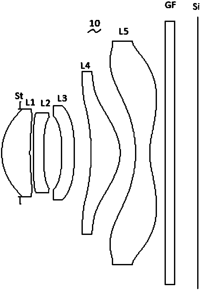
[0025] Referring to the accompanying drawings, the present invention provides an imaging optical lens. figure 1 Shown is an imaging optical lens 10 according to a first embodiment of the present invention, and the imaging optical lens 10 includes five lenses. Specifically, the imaging optical lens 10 sequentially includes, from the object side to th...


PUM


Abstract

The invention relates to the field of optical lenses and discloses an imaging optical lens successively comprising, from an object side to an image side, an aperture, a first lens, a second lens, a third lens, a fourth lens, and a fifth lens. The material of the third lens is glass. The material of the first lens, the second lens, the fourth lens, and the fifth lens is plastic. The imaging opticallens satisfies the following relation: 0.83<f1/f<0.87, 2.9<f2/f< 2.7, 8.3<f3/f< 8.0, 0.55<f4/f<0.65, and 0.55<f5/f<-0.45. The imaging optical lens can satisfy the requirements of high pixels and large image heights while better correcting most optical aberrations of an optical system.

Description

technical field [0001] The invention relates to the field of optical lenses, in particular to an imaging optical lens. Background technique [0002] In recent years, with the rise of smart phones, the demand for miniaturized photographic lenses is increasing, and the photosensitive devices of general photographic lenses are nothing more than Charge Coupled Device (CCD) or Complementary Metal Oxide Semiconductor Device (Complementary Metal Semiconductor). -OxideSemicondctor Sensor, CMOS Sensor), and due to the improvement of semiconductor manufacturing technology, the pixel size of the photosensitive device has been reduced, and the current electronic products have good functions, thin and short appearance as the development trend, so it has good The miniaturized camera lens with imaging quality has become the mainstream in the current market. [0003] In order to obtain better image quality, the lenses traditionally mounted on mobile phone cameras mostly adopt a three-piece...

Claims


Application Information

Patent Timeline
Patent Type & Authority Applications(China)
IPC IPC(8): G02B13/00G02B13/18
CPCG02B13/0045G02B13/18
Inventor 王建明
Owner AAC ACOUSTIC TECH (SHENZHEN) CO LTD
Why Eureka
Try Eureka