Refrigerator including touch sensor
A touch sensor, sensor technology, applied in the input/output process of instruments, data processing, household refrigeration devices, etc., can solve the problems of insufficient sensing speed and response speed of touch operation, etc.
Active Publication Date: 2018-03-13
LG ELECTRONICS INC
4 Cites 0 Cited by
AI-Extracted Technical Summary
Problems solved by technology
In these cases, the sensing speed and response speed...
Method used
[0072] As described above, the number display portion 11a and the symbol display portion 11b forming the display area 11 may be formed of the first through hole 21 having a miniature size, and a portion toward which light is not emitted may be difficult to recognize from the outside. Therefore, other components are not arranged on the front exterior of the refrigerator door 10 , and the overall front exterior of the refrigerator door 10 provides simple and luxurious aesthetics by giving a feeling of being formed of a metal plate due to the front panel 20 .
[0073] In some embodiments, the first through hole 21 may be filled with a sealing member 22. The sealing member 22 prevents the first through hole 21 from being clogged with foreign matter. The sealing member 22 is formed of a silicone or epoxy material, and may be formed of a material capable of sealing the first through hole 21 while light may pass therethrough. In some embodiments, since the inside of the first through hole 21 is filled with the sealing member 22, the processed surface of the first through hole 21 may be prevented from being corroded.
[0092] In some embodiments, the board support part 140 on which the support board 141 is mounted is formed at both left and right ends of the top of the frame 100. The support plate 141 is installed in an area of an upper space of the frame 100 corresponding to the top of the cover display 200 while the cover display 200 is installed, and is configured to support the front panel 20 from the rear. Therefore, not only heave of the corresponding portion of the front panel 20 but also deformation of the front panel 20 caused by external impact can be prevented.
[0117] All the cover combining parts 516 and the main body combining parts 521 are arranged at equidistant intervals and arranged at the same position on the left and right sides to face each other, so that the connection between the case cover 510 and the case main body 520 is simultaneously achieved by the same power. combination, thus preventing the resilient member 720 from tilting during the assembly process.
[0131] In some embodiments, the installation location of the elastic member 720 (eg, the location where the display portion 715 is installed) may be positioned both to the left and right of the location of the sensor 750 (as seen in FIG. 17 ). In some embodiments, the installation location of the elastic member 720 (eg, the location where the display portion 715 is installed) may be positioned further outside than the outer end of the sensor 750 . The sensor 750 may be configured not to interfere with the elastic member 720 due to the elastic member 720 to prevent the detection capability of the sensor 750 from being lowered. In some examples, a plurality of elastic members 720 may be equidistantly spaced from the sensor 750 to provide the same pressure on the sensor PCB 700 .
[0137] The guide portions are the through holes 7...
Abstract
A refrigerator includes a door that has a front panel with an operation area to receive a touch operation of a user; a touch sensor assembly that is located rearward the operation area and that includes sensors to generate an input signal based on the touch operation; and a sensor controller connected to the touch sensor assembly and configured to process the input signal received from the touch sensor assembly. The sensor controller is configured to determine whether the touch operation is a push operation or a release operation based on comparison of a voltage value of the processed input signal to predetermined first and second threshold voltage values.
Application Domain
Lighting and heating apparatusElectronic switching +4
Technology Topic
EngineeringVoltage +4
Image
Examples
- Experimental program(1)
Example Embodiment
[0051] The above objects, features and advantages will be described in detail below to allow those skilled in the art to easily implement the technical concept of the present disclosure with reference to the accompanying drawings. In descriptions of embodiments of the present disclosure, some detailed explanations of well-known functions or components in the related art will be omitted when it is considered that the well-known functions or components may unnecessarily obscure the essence of the present disclosure. Hereinafter, exemplary embodiments of the present disclosure will be described in detail with reference to the accompanying drawings. Throughout the drawings, the same reference numbers refer to the same or similar elements.
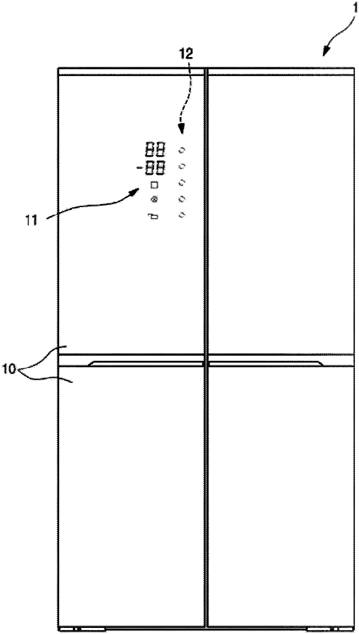
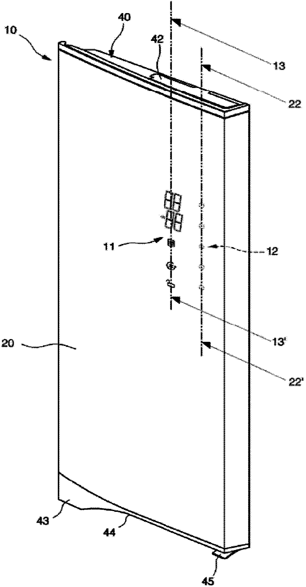
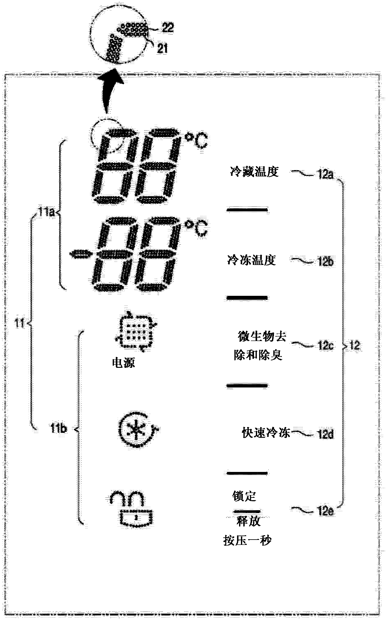
[0052] For convenience of description, embodiments of the present disclosure will be described by taking a side-by-side refrigerator as an example. However, the present disclosure is applicable not only to other types of refrigerators than the side-by-side refrigerator, but also to other electronic devices to which the touch interface is applicable.
[0053] figure 1 is a front view showing an exemplary refrigerator.
[0054] as in figure 1 As shown in , the outer shape of the exemplary refrigerator 1 may be formed by a cabinet forming a storage space and a refrigerator door 10 mounted on the cabinet to open and close the storage space.
[0055] The storage space may be divided into left and right sides and/or top and bottom, and a plurality of such refrigerator doors 10 that open and close each space may be provided at the open front side of the storage space. The refrigerator door 10 may be configured to slidably or rotatably open and close a storage space, and may define a front outer shape of the refrigerator 1 in a closed state.
[0056] In some instances, the display area 11 and the operation area are provided at the refrigerator door 10 on one side among the plurality of refrigerator doors 10 at a height that allows the user to easily operate and appreciate.
[0057] The display area 11 is an area for externally displaying the operation state of the refrigerator 1, and light emitted from the inside of the refrigerator door 10 passes through the display area 11 and displays symbols or numbers to allow for inspection from the outside. Here, the display area 11 may be defined to include holes and transparent portions through which light can pass.
[0058] The operation area is a part including a plurality of touch parts 12 that the user touches to operate the refrigerator 1, is provided in a partial area of the front side of the refrigerator door 10, and includes various methods (including surface treatments such as printing and etching or light transmission) that can be used. ) is used to sense the part of the pressing operation.
[0059] figure 2 is a perspective view of an exemplary refrigerator door, image 3 is a view illustrating a display area and an exemplary operating area of a refrigerator door, Figure 4 is an exploded perspective view illustrating an exemplary mounting structure of an exemplary display assembly of a refrigerator door, and Figure 5 is an exploded perspective view illustrating an exemplary front panel separated from a refrigerator door.
[0060] As shown in the figures, the general outer shape of the refrigerator door 10 includes: a front panel 20, which generally forms an outer shape; decorative members 40 and 43, which are provided at the top and bottom ends of the front panel 20; And the door liner 30 that forms the rear outer shape of the refrigerator door 10 .
[0061] In more detail, the front panel 20 forms the front outer shape of the refrigerator door 10, and may be formed of stainless steel in a flat shape. In some embodiments, the front panel 20 is a component that forms at least a portion of the exterior shape of the refrigerator door 10 and may be referred to as an exterior member in other household appliances other than refrigerators.
[0062] The front panel 20 may be formed of metal or a material having a texture similar to that of metal instead of stainless steel, and, if necessary, may be formed of glass or plastic material.
[0063] The front panel 20 may form not only a front surface of the refrigerator door 10 but also a part of a side surface of the refrigerator door 10 if necessary, and may further perform anti-fingerprint processing or hairline processing on the surface of the front panel 20 .
[0064] In some embodiments, the display area 11 may be defined by a plurality of first through holes 21 arranged in a partial area of the front panel 20 . The display area 11 may form a number display part 11a displaying numbers and a symbol display part 11b displaying symbols, letters or figures using a set of a plurality of first through holes 21 perforated in certain arrangements.
[0065] For example, the digital display portion 11a may be formed by arranging a plurality of sets of the first through holes 21 in a seven-segment shape. The digital display portion 11a may be provided at each of the top and bottom to independently display the temperatures of the refrigerating compartment and the freezing compartment. The digital display section 11a can display another piece of information that can be displayed as a number in addition to the temperature information, and different pieces of information can be selectively displayed by operating on the operation area.
[0066] In some embodiments, the symbol display portion 11b may be formed under the numeral display portion 11a. The symbol display part 11b may display the operation state of the refrigerator 1 as a symbol or a figure, and is formed by arranging a set of the first through holes 21 in a shape corresponding to the operation state to allow the user to know the operation state intuitively.
[0067] For example, in image 3 Among the symbol display sections 11b, the symbol display section 11b positioned at the uppermost may be displayed in a lock shape to indicate a locked state, and the symbol display section 11b positioned in the middle may be displayed in a filter shape to indicate a microorganism removing function or a deodorizing function , and the symbol display portion 11b positioned at the lowermost portion may be displayed in the shape of a rotating fan to indicate the quick freezing function. The shape of the symbol display portion 11b may be various, and the number thereof may be various.
[0068] The display area 11 may be formed to correspond to the arrangement of the second through holes 220 and the third through holes 321 , which will be described below as transmitting light emitted from light emitting diodes (LEDs) of the display assembly 300 . The first through hole 21 is formed to have a micro size by laser processing or etching, and may have a size that is not easily discernible from the outside in a state where light passes therethrough.
[0069] Even if the numeral display portion 11a and the symbol display portion 11b include a plurality of first through holes 21 in the shape shown in image 3 However, due to the miniature size of the first through-holes 21, it may be difficult to visually recognize the LEDs 313 when they are not turned on in a state spaced at a certain distance.
[0070] That is, in the case of the digital display portion 11a, only the portion toward which light is emitted depending on the operation of the seven segments passes through the first through holes 21 to display numbers on the front panel 20, and no light is emitted toward it. Parts are not well identified.
[0071] In some instances, in the case of the symbol display portion 11b, since light is emitted when the LED 313 corresponding to the function is turned on, the symbol display portion 11b can be recognized from the outside, but is not well recognized when the LED 313 is turned off identify.
[0072] As described above, the numeral display portion 11a and the symbol display portion 11b forming the display area 11 may be formed of the first through holes 21 having a micro size, and portions toward which light is not emitted may be difficult to recognize from the outside. Therefore, other components are not arranged on the front exterior of the refrigerator door 10 , and the overall front exterior of the refrigerator door 10 provides a simple and luxurious aesthetic by giving a feeling of being formed of a metal plate due to the front panel 20 .
[0073] In some embodiments, the first through hole 21 may be filled with the sealing member 22 . The sealing member 22 prevents the first through hole 21 from being blocked with foreign matter. The sealing member 22 is formed of a silicone or epoxy material, and may be formed of a material capable of sealing the first through hole 21 while light can pass therethrough. In some embodiments, since the inside of the first through hole 21 is filled with the sealing member 22, the machined surface of the first through hole 21 can be prevented from being corroded.
[0074] The sealing member 22 may fill the inside of the first through hole 21 through an additional process, and may be configured to fill the first through hole 21 or be attached as a sheet to block a plurality of first through holes simultaneously during a surface coating process of the front panel 20 . A through hole 21 . That is, the fingerprint coating solution and/or the diffusion sheet in the front panel 20 may function as the sealing member 22 .
[0075] The operation area is a portion displayed to allow the user to perform a touch operation, and may include a plurality of touch portions 12 . Accordingly, the touch portion 12 displays an area that can be sensed by the touch sensor assembly 500 when the user touches the area of the touch portion 12 .
[0076] The touch portion 12 is not a physical button, and designates an area displayed on the front surface of the front panel 20 . The sensor 750 in contact with the rear surface of the front panel 20 can be operated by operating the displayed area.
[0077]The touch portion 12 may be displayed on the front surface of the front panel 20 by etching, printing or other surface treatment, and may be displayed so as not to be significantly visible from the outside to be seen so that the overall texture of the front panel 20 forms the exterior. In some embodiments, the touch portions 12 may be displayed as letter or symbol shapes to allow the user to intuitively understand and operate the corresponding function of each touch portion 12 . In some embodiments, the touch portion 12 may display a recognizable area when a user performs a touch operation, and is configured to effectively recognize when the displayed portion is pressed.
[0078] The door liner 30 is combined with the front panel 20 and forms a surface facing the interior of the storage space. The door liner 30 is injection molded using a plastic material and can provide a structure in which the liner is positioned along the perimeter of the structure and on which the basket can be mounted. In some embodiments, the door liner 30 when combined with the front panel 20 forms a space between the door liner 30 and the front panel 20 , and the space can be filled with a foam solution that forms the insulator 24 .
[0079] The frame 100 may be attached to the rear surface of the front panel 20 . The frame 100 is formed to provide an extra space in the refrigerator door 10 that is not filled with the foam solution, and to provide spaces in which the cover display 200 , the display assembly 300 , the touch sensor assembly 500 , the frame display 400 and the like are accommodated.
[0080] The trim members 40 and 43 form upper and lower exteriors of the refrigerator door 10 and are configured to shield open upper and lower ends of the refrigerator door 10 and are formed between the front panel 20 and the door lining 30 by being combined.
[0081] Among the decorative members 40 and 43 , the decorative member 40 at the upper portion of the refrigerator door 10 includes an inlet 41 and an inlet cover 42 which opens and closes the inlet 41 . The inlet 41 passes through the decorative member 40 and is connected to the space formed by the frame 100 . Therefore, a user can insert the frame display 400 assembled with the display assembly 300 through the inlet 41 . To this end, the inlet 41 is formed to have a size that allows the frame display 400 to be inserted therein, and can be positioned vertically above the cover display 200 .
[0082] In some embodiments, a hinge hole is formed in one side of the trim member 40 , and the hinge in the hinge hole becomes the pivot of the refrigerator door 10 . In some embodiments, a structure is provided in which the guided wires can be moved in and out inside the frame 100 through the hinge holes and can be connected to the power supply portion of the cabinet.
[0083] A door handle 44 may be provided at the trim member 43 at the lower portion of the refrigerator door 10 . The door handle 44 is recessed in a notch shape and is configured to operate to pivot the refrigerator door 10 . A lever 45 for opening and closing the refrigerator door 10 is further provided at the trim member 43 at the lower portion of the refrigerator door 10 . The latch assembly 31 is actuated by operating the lever 45 to select whether the refrigerator door 10 remains in the open mode or the closed mode.
[0084] The cover display 200 is attached to the rear surface of the front panel 20 . The cover display 200 serves to guide the display assembly 300 to be mounted (the LED 313 is mounted on the display assembly 300 ), and is configured to be attached using a double-sided tape or an adhesive member 25 formed by applying a primer to the rear surface of the front panel 20 .
[0085] A touch sensor assembly 500 capable of sensing a user's pressing operation on the front panel 20 is installed on one side of the cover display 200 . The cover display 200 has a structure capable of being attached to the front panel 20 while being combined with the touch sensor assembly 500 .
[0086] The cover display 200 may be attached at a position of the display area 11 corresponding to the second through hole 220 formed in the cover display 200 . In some embodiments, the cover display 200 is housed in the frame 100 while being attached.
[0087] In some embodiments, the display assembly 300 is inserted into the space in the frame 100 through the inlet 41 while being mounted on the frame display 400 . When the frame display 400 is fully inserted, the display assembly 300 is positioned within the cover display 200 and light emitted from the LEDs 313 can pass through the cover display 200 and the display area 11 and be emitted outward.
[0088] Image 6 is an exploded perspective view illustrating the combined structure of the touch sensor assembly, the cover display, the display assembly, the frame display, and the frame. Figure 7 is shown along the Figure 4 A cross-sectional view of the portion taken on line 7-7', and Figure 8 is shown along the Figure 4 A cross-sectional view of the section taken on line 8-8'.
[0089] As shown in the figures, the frame 100 is formed to have an open front surface and an open top surface, and when attached to the front panel 20, a space 110 having an open top surface is formed. To this end, except for the top end of the frame 100 , the periphery of the frame 100 is bent toward the front panel 20 , and the ends thereof are bent toward the outside again to form the frame adhesive portion 120 . The adhesive member 25 formed of double-sided tape or adhesive is provided at the frame adhesive portion 120 in such a manner that the frame 100 can be attached to the rear surface of the front panel 20 .
[0090] The top end of the frame 100 comes into contact with the bottom surface of the decoration member 40 while the frame 100 is attached to the front panel 20 . Therefore, the open top surface of the frame 100 may be interconnected with the inlet 41 and form an independent space in the refrigerator door 10 .
[0091] Therefore, even when the foam solution for forming the insulator 24 is injected into the refrigerator door 10, the foam solution may not flow into the space in the frame 100, and the space may be protected. In some embodiments, a plurality of reinforcing ribs 130 are formed on the rear surface of the frame 100 to cross each other longitudinally and laterally. Due to the reinforcing ribs 130, even when the foam solution for forming the insulator 24 is filled with a high pressure, the space in the frame 100 can be maintained without deformation.
[0092] In some embodiments, the plate support portion 140 (on which the support plate 141 is mounted) is formed at both the left and right ends of the top of the frame 100 . The support plate 141 is installed in an area of the upper space of the frame 100 corresponding to the top of the cover display 200 while the cover display 200 is installed, and is configured to support the front panel 20 from the rear. Therefore, it is possible to prevent not only heave of the corresponding portion of the front panel 20 but also deformation of the front panel 20 caused by an external impact.
[0093] The plate supporter 140 is formed in a stepped shape, and is configured to support both ends of the support plate 141 . In some embodiments, the support plate 141 is slidably inserted into the space between the plate support 140 and the front panel 20 when the frame 100 is attached to the front panel 20 . The support plate 141 may be attached to the rear surface of the front panel 20 when attached to the frame 100 while both ends thereof are fixed to the plate supporter 140 .
[0094] The wire port 150 is formed at the top of the side surface of the frame 100 . The wire ports 150 form a path for allowing wires to pass through which connect the electronic components provided in the frame 100 to the power supply on the cabinet. The wire port 150 may be formed at the top of the side surface close to the hinge of the refrigerator door 10 and disposed close to the hinge hole of the refrigerator door 10 . In some embodiments, the wire port 150 may be done when the foam solution is injected into the refrigerator door 10 to prevent the foam solution from penetrating the frame 100 .
[0095] In some embodiments, the fastening grooves 160 are formed in both the left and right sides of the frame 100 . The fastening grooves 160 are formed to allow the fastening portions 230 protruding laterally from both the left and right ends of the cover display 200 to be inserted therein. That is, the fastening groove 160 is recessed toward the outside, and is formed in a shape corresponding to the fastening portion 230 in such a manner that the cover display 200 does not move to be held in a precise position.
[0096] A cover supporter 170 that supports the cover display 200 is formed at a portion below the fastening groove 160 where the cover display 200 is positioned. The cover supporters 170 protrude from the left and right sides of the frame 100 and may push and support both the left and right ends of the cover display 200 .
[0097] Therefore, when the frame 100 is attached to the front panel 20 and the foam solution is injected into the refrigerator door 10 while the cover display 200 is attached to the rear surface of the front panel 20, the cover supporter 170 pushes the cover display 200 forward to The cover display 200 is allowed to remain in a state of being attached to the front panel 20 . For example, even when the adhesive member 25 attaching the cover display 200 to the front panel 20 is cured and loses its function, the cover support 170 may press the cover display 200 to allow the front panel 20 and the cover display 200 to remain in contact with each other in close contact.
[0098] A plurality of such cover supports 170 are vertically arranged at certain intervals to push the entire cover display 200 evenly for support. In some embodiments, a forwardly protruding protrusion 171 is formed further in front of the cover support 170 adjacent to the cover display 200 . The protrusions 171 are formed in a rib shape or a protrusion shape elongated in the lateral direction, and may make linear contact or point contact with the cover display 200 . Therefore, even when the contact surface between the cover display 200 and the cover supporter 170 is uneven, the cover display 200 is not inclined and each cover supporter 170 can transmit uniform pressure to the cover display 200 .
[0099] The cover display 200 is formed of a plastic material in a flat shape, and is formed to be accommodated in the frame 100 while being attached to the front panel 20 . In some embodiments, fastening portions 230 that protrude outward and are inserted into the fastening grooves 160 are formed at the tops of left and right ends of the cover display 200 .
[0100] In some embodiments, the receiving portion 210 on which the touch sensor assembly 500 is mounted is formed in the cover display 200 . In some implementations, a plurality of such second through holes 220 are formed in the cover display 200 at positions corresponding to the display area 11 .
[0101] The display assembly 300 may include: a display printed circuit board (PCB) 310 on which the LEDs 313 are mounted; and a reflector 320 disposed in front of the display PCB 310 .
[0102] Figure 9 is a front exploded perspective view illustrating the touch sensor assembly. Figure 10 is a rear exploded perspective view illustrating the touch sensor assembly.
[0103] As shown, touch sensor assembly 500 may include: a sensor housing forming an overall outer shape; a sensor PCB 700 in which the sensor PCB 700 is housed; a resilient member 720 supporting the sensor PCB 700; and a touch Booster 530, touch booster 530 is combined with the open front surface of the sensor housing.
[0104] The sensor housing may include a housing cover 510 and a housing body 520 assembled to form a space in which the sensor PCB 700 is accommodated.
[0105] The housing cover 510 forms the front half of the sensor housing, and housing assembly portions 511 are formed at the top and bottom ends of the housing cover 510 to allow the touch sensor assembly 500 to be mounted on the cover display 200 . In some embodiments, the housing cover 510 may expose the front surface while the touch sensor assembly 500 is mounted on the receiving portion 210 and may be attached to the rear surface of the front panel 20 using the adhesive member 25 .
[0106]An opening 512 is formed in the front surface of the housing cover 510 , and a touch booster 530 is installed in the opening 512 . The touch booster 530 is used to transmit the displacement of the front panel 20 generated when the user presses the front panel 20 to the sensor 750 which will be described below, and the detailed structure will be described in detail again below.
[0107] The opening 512 may be formed to have a size corresponding to the size of the touch booster 530, and may be shielded by the touch booster 530 when the touch booster 530 is installed. Rearwardly extending extension ribs 517 are formed on the perimeter of the opening 512 and are formed to make contact with the perimeter of the sensor PCB 700 to guide the sensor PCB 700 without tilting as the sensor PCB 700 moves forward and backward move.
[0108] In some examples, a booster support 513 formed to protrude inwardly and extend rearward may be further formed on the interior of the opening 512 . When the touch booster 530 is installed, the booster supporter 513 supports the periphery of the touch booster 530 from the rear to prevent the touch booster 530 from moving toward the touch booster 530 even when pressure is applied to the touch booster 530 . then move farther than the set position.
[0109] A booster support 513 may be formed along the opening 512 and a hook groove 514 is formed in the booster support 513 . The hook groove 514 is formed at a position corresponding to the hook 531 of the touch booster 530 , and may be formed by partially cutting the booster supporter 513 . The hook groove 514 may be independently formed in one side of the housing cover 510 adjacent to the opening 512 not at the booster support 513 .
[0110] The hooks 531 and the hook grooves 514 are formed at positions facing each other on both the left and right sides, and are arranged at certain intervals in the vertical direction to prevent the touch booster 530 from being touched when the touch booster 530 is operated Lean in one direction.
[0111] In some examples, hook slot 514 is formed lengthwise in forward and rearward directions, and is formed to allow hook 531 to move in the forward and rearward directions while being positioned inside hook slot 514 . Therefore, the touch booster 530 may remain in the combined state with the housing cover 510, but may move some distance in the forward and backward directions. In some instances, touch booster 530 protrudes to allow its front surface to be further forward than housing cover 510 while being assembled in housing cover 510 . Therefore, when the touch sensor assembly 500 and the cover display 200 are attached to the front panel 20 , the touch booster 530 may be kept in a state of being in constant contact with the rear surface of the front panel 20 .
[0112] In some embodiments, the cover assembly portion 516 may be formed on the peripheral surface of the housing cover 510 . The cover combining part 516 is a part that is combined in shape with the main combining part 521 which is formed at the housing body 520 and may be formed in the shape of a groove or hole capable of holding and fastening the hook-shaped cover combining part 516 . Here, it is necessary to form the cover combining part 516 at a position where the elastic member 720 can be compressed when the cover combining part 516 and the main body combining part 521 are fastened to each other.
[0113] That is, when the case cover 510 and the case body 520 are combined with each other, the elastic member 720 is compressed to push the sensor PCB 700 and the touch booster 530 forward. Therefore, the touch booster 530 may always protrude and remain in a state of being in close contact with the front panel 20, and may effectively sense a user's pressing operation on the front panel 20.
[0114] In some examples, wire holes 515 are formed in the top surface of housing cover 510 . The wire holes 515 are open to allow the first cable connectors 610 connected to the sensor terminals 711 mounted on the sensor PCB 700 to move in and out therethrough. The wire hole 515 may be formed in at least any one of the case cover 510 and the case body 520 .
[0115] The housing body 520 may be combined with the housing cover 510 to form the outer shape of the rear half of the touch sensor assembly 500 and form a space in which the sensor PCB 700 may be installed.
[0116] A plurality of such main body combining parts 521 are formed on a peripheral surface that is curved forward along the periphery of the housing main body 520 . The body combining part 521 may be formed by partially cutting the peripheral surface of the housing body 520 and inserted into the cover combining part 516 to allow the housing cover 510 and the housing body 520 to remain in a state of being combined with each other.
[0117] All the cover combination parts 516 and the main body combination parts 521 are arranged at equal intervals and at the same positions on the left and right sides facing each other to simultaneously achieve the combination between the housing cover 510 and the housing body 520 by the same power, so The elastic member 720 is prevented from tilting during the assembly process.
[0118] In some embodiments, wire holes 522 may be formed on the top surface of the perimeter of the housing body 520 . A wire hole 522 may be formed at the same location as the position of the wire hole 515 of the housing cover 510 to allow the first cable connector 610 to move in and out therethrough.
[0119] Mounting guides 523 may be formed at the bottom surface of the housing body 520 . The mounting guide 523 may guide a plurality of such elastic members 720 and may be formed to accommodate the elastic members 720 attached to the sensor PCB 700 .
[0120] The mounting guide 523 may be formed in a shape corresponding to the shape of the sensor PCB 700 , and may form a space corresponding to the lateral width of the elastic member 720 . Therefore, the elastic member 720 may be positioned in the inner area of the mounting guide 523 , and both left and right surfaces of the mounting guide 523 support both left and right ends of the elastic member 720 . Therefore, although the elastic member 720 is compressed, it may be possible to stably support the elastic member 720 without being distorted or inclined in one direction.
[0121] In some examples, the terminal holes 524 may be formed to open in the bottom surface of the housing body 520 corresponding to the sensor terminals 711 provided at the sensor PCB 700 . The terminal hole 524 may be formed in a shape corresponding to the sensor terminal 711 , and may be formed to pass through the terminal hole 524 to expose the sensor terminal 711 . Therefore, the sensor terminal 711 may not interfere with the bottom of the housing body 520 even when the sensor PCB 700 is moved forward and backward.
[0122] In some embodiments, since the first cable connector 610 may be combined with the side surface of the sensor terminal 711 , it may be possible to check the combined state between the first cable connector 610 and the sensor terminal 711 through the terminal hole 524 .
[0123] In some embodiments, the sensor PCB 700 may be supported in the sensor housing by the elastic member 720 while the spacer 730, the sensor 750, and the conductive foil 740 are disposed thereon. In some embodiments, the touch booster 530 can be mounted in the opening 512 to be movable forward and backward, and can contact the front panel 20 and the conductive foil 740 to immediately transmit the movement generated when a pressing operation is performed on the sensor 750 . bit.
[0124] Figure 11 is a longitudinal cross-sectional view of the touch sensor assembly. In some embodiments, Figure 12A and Figure 12B It is a plan and rear view of the sensor PCB which is an important part of the touch sensor assembly. Figure 13 is a plan view of the spacer that is an important part of the touch sensor assembly. In some embodiments, Figure 14 is a plan view of the conductive foil that is an important part of the touch sensor assembly.
[0125] In some embodiments, the sensor PCB 700 may be formed of a plastic material, and the copper film 712 forming the circuit may be printed on its surface. In some embodiments, a sensor 750 that senses a pressing displacement of the front panel 20 caused by a user's touch may be disposed on the front surface of the sensor PCB 700 .
[0126] Sensor 750 may be formed of a piezoelectric sensor. For example, sensor 750 may be formed by attaching ceramic element 752 to the top surface of metal plate 751 . The metal plate 751 may be elastically deformed according to the pressure of the user's touch operation on the front panel 20, and the ceramic element 752 generates a change in electric quantity caused by the pressure. In some embodiments, sensor 750 has been described as being formed, for example, in a circular shape. However, the sensor 750 is not limited to a circular shape, and may be formed in various shapes.
[0127] In some embodiments, a plurality of such sensors 750 may be formed along the sensor PCB 700, and the sensor support 713 is formed on the front surface of the sensor PCB 700 on which the sensors 750 are mounted.
[0128] The sensor supporter 713 may be defined by a groove having a diameter smaller than that of the sensor 750 , and is formed to support the periphery of the sensor 750 , and more precisely the periphery of the metal plate 751 , from below. That is, the sensor supporter 713 has the feature of supporting the periphery of the metal plate 751 . Therefore, the sensor supporter 713 may be formed in the shape of the protrusion supporting the periphery of the metal plate 751 instead of the shape of the groove. In some embodiments, the size of the sensor support 713 may be smaller than the diameter of the metal plate 751 and larger than the diameter of the ceramic element 752 . Therefore, the metal plate 751 can be deformed by the pressure applied from the front, and the ceramic element 752 can effectively sense the change in pressure.
[0129] In some embodiments, a common contact 714 connected by the plurality of sensors 750 and the positive pole of the circuit can be formed in one side of the sensor PCB 700 . The common contact point 714 is configured to connect the bottom surface of the plurality of sensors 750 and to make contact with the conductive traces 741 of the conductive foil 740 and connect to the negative terminal of the plurality of sensors 750 when the conductive foil 740 is glued to allow the sensors 750 to be Conductive.
[0130] A mounting display portion 715 showing the precise mounting position of the elastic member 720 may be formed on the rear surface of the sensor PCB 700 . The installation display portion 715 may be formed by printing or processing, and is configured to indicate a position where the elastic member 720 is installed.
[0131] In some embodiments, the installation location of the elastic member 720 (eg, the location where the display portion 715 is installed) may be positioned both to the left and to the right of the location of the sensor 750 (from Figure 17 seen). In some embodiments, the mounting location of the resilient member 720 (eg, where the display portion 715 is mounted) may be positioned further outward than the outer end of the sensor 750 . The sensor 750 may be provided so as not to interfere with the elastic member 720 due to the elastic member 720 to prevent the detection capability of the sensor 750 from being lowered. In some instances, a plurality of elastic members 720 may be spaced equidistantly from the sensor 750 to provide the same pressure to the sensor PCB 700 .
[0132] In some embodiments, the positions of the plurality of sensors 750 may be arranged on the same extension line as the extension line of the body assembly portion 521 and the cover assembly portion 516 . That is, if in Figure 14As shown, the body assembly portion 521 and the cover assembly portion 516 may be positioned on the same extension line on both the left and right sides of the sensor 750 . In some embodiments, the body combination portion 521 and the cover combination portion 516 may be arranged to be positioned between a pair of such resilient members 720 adjacent the sensor 750 . Therefore, on the left and right sides of the sensor 750, the main body combining part 521 and the cover combining part 516 are positioned, and the pair of elastic members 720 are positioned in a direction crossing the same. All of the plurality of main body combining parts 521 , cover combining parts 516 , and elastic members 720 are configured to be arranged as described above. Due to this, pressure can be uniformly applied to the overall sensor PCB 700 positioned in the sensor housing, and all the plurality of sensors 750 can sense the user's operation signal under the same conditions.
[0133] In some embodiments, spacer 730 is attached to the front surface of sensor PCB 700 . The spacer 730 serves to bond the sensor PCB 700 and the conductive foil 740 to each other, and may be formed of an adhesive member such as double-sided tape. The spacer 730 is formed to have a size corresponding to the size of the sensor PCB 700 and the conductive foil 740 . In some embodiments, the spacers 730 may be formed with a certain thickness to allow the conductive foil 740 to make contact with the top surface of the sensor 750 and the common contact point 714 at a sufficient height.
[0134] In some embodiments, the sensor hole 731 may be formed at a position corresponding to the position of the sensor 750 by perforating. The sensor hole 731 is formed to be larger than the size of the sensor 750 to accommodate the sensor 750 therein without interfering in the operation of the sensor 750 . In some embodiments, the number of such sensor holes 731 corresponds to the number of sensors 750 , and vent holes 732 cut to lengths are formed at each sensor hole 731 .
[0135] The ventilation holes 732 for discharging air bubbles generated when the spacer 730 is attached may be formed along the longitudinal direction of the spacer 730 , and all the ventilation holes 732 may extend in one direction. Here, the spacer 730 may be gradually attached in a direction in which the ventilation hole 732 extends from the sensor hole 731 .
[0136] In some embodiments, guide portions are provided at the spacer 730 and the conductive foil 740 to attach the spacer 730 and the conductive foil 740 at precise locations.
[0137] For example, the guide portions are through holes 733 and 744 provided at the spacer 730 and the conductive foil 740 . A plurality of such through holes 733 and 744 may be formed along the spacer 730 and the conductive foil 740 and alternately arranged. In some embodiments, levers are provided at the sensor PCB 700 at positions corresponding to the through holes 733 and 744 to sequentially attach the spacer 730 and the conductive foil 740 through the corresponding through holes 733 and 744 . The spacer 730 and the conductive foil 740 may be attached at precise positions due to the guide portion and kept at precise intervals from the sensors 750 provided at the sensor PCB 700 to prevent errors generated by the plurality of sensors 750 .
[0138] The conductive foil 740 may be formed of a resin film material such as PET, and may be formed to have a size corresponding to the size of the sensor PCB 700 and the spacer 730 . In some embodiments, a mesh-shaped conductive trace 741 capable of connecting all top surfaces of the plurality of sensors 750 and the common contact point 714 is formed at the conductive foil 740 . Conductive traces 741 are printed on the bottom surface of conductive foil 740 using a silver material, and the surface on which conductive traces 741 are printed makes contact with spacers 730 and at the same time with sensor 750 and common contact 714 .
[0139] In some embodiments, inner guide lines 742 and outer guide lines 743 are printed on conductive foil 740 to attach sensors 750 at precise locations. The inner guide line 742 is formed to correspond to the size of the ceramic member 752 , and the outer guide line 743 is formed to correspond to the size of the metal plate 751 . Therefore, when the sensor 750 is mounted at a precise position, the ceramic element 752 is positioned on the inner guide line 742 and the metal plate 751 is positioned on the outer guide line 743 . In some embodiments, conductive traces 741 having a grid or mesh shape connect the common contact point 714 to the top surface (eg, negative electrode) of the sensor 750 to allow the sensor 750 to be conductive.
[0140] Figure 15 is a rear perspective view of the touch booster, which is an important part of the touch sensor assembly.
[0141] As shown in the figure, the touch booster 530 is formed to have a size corresponding to the size of the opening 512 of the housing cover 510 to cover the opening 512 . In some embodiments, hooks 531 are formed on both the left and right ends of housing cover 510 . The hooks 531 are combined with the hook grooves 514 formed at the housing cover 510, and a plurality of such hooks 531 are formed at certain intervals. In some embodiments, hook 531 is formed to be movable forward and rearward in hook slot 514 .
[0142] In some embodiments, a plurality of elastically deformable portions corresponding to the number of sensors 750 are formed at touch booster 530 . The elastically deformable portion is formed at a position corresponding to the positions of the touch portion 12 of the front panel 20 and the sensor 750, and has an elastically deformable structure to be movable forward and backward. Therefore, when the user presses the touch portion 12, the portion corresponding to the area of the touch portion 12 moves backward according to the deformation of the front panel 20, and the sensor 750 may be pressurized. In some embodiments, the elastically deformable portion is configured to return to the original position when the user removes the hand from the touch portion 12 .
[0143] For example, the elastically deformable part may include: a first extension part 532 extending from one side of the open area of the touch booster 530; a second extension part 533 extending from the first extension part 533 and a common portion 534, which is provided in the center to connect the first extending portion 532 and the second extending portion 533.
[0144] The first extension portion 532 and the second extension portion 533 are formed to have a relatively small width to allow the common portion 534 to be movable, and are extended to have a sufficient length to be easily elastically deformed while being bent at least once. The first extension part 532 and the second extension part 533 are curved along the circumference of the common part 534 and may be formed symmetrical based on the common part 534 . In some embodiments, areas other than the first extension portion 532, the second extension portion 533, and the common portion 534 are helically cut toward the center of the common portion 534 to form a cut portion 536, and may be cut along the first extension The peripheries of the portion 532, the second extension portion 533 and the common portion 534 are curved.
[0145] In some embodiments, downwardly protruding protrusions 535 are formed at the bottom surface of the common portion 534 . The protrusion 535 is positioned at the center of the common portion 534 at a position corresponding to the center of the sensor 750 . Therefore, when the common portion 534 is moved rearward, the center of the sensor 750 may be pressurized.
[0146] Figure 16 is a cross-sectional view illustrating a touch sensor assembly mounted on a refrigerator door.
[0147] As shown in the figure, the touch sensor assembly 500 is attached to the front panel 20 while being mounted on the cover display 200 . Here, the adhesive member 25 is attached to the front surface of the cover display 200 and the front surface of the housing cover 510 to bond the cover display 200 and the touch sensor assembly 500 to the rear surface of the front panel 20 .
[0148] Here, the adhesive member 25 is not provided at the touch booster 530 , and the touch booster 530 comes into contact with the rear surface of the front panel 20 . To this end, when the touch sensor assembly 500 is assembled, the elastic member 720 is compressed and pushes the sensor PCB 700 forward. Thus, the sensor PCB 700 makes contact with the touch booster 530 . The touch booster 530 is movable forward and backward while being combined with the housing cover 510 , and is configured to protrude further forward than the front surface of the housing cover 510 due to the pressure applied by the elastic member 720 .
[0149] In some instances, even when the cover display 200 and the housing cover 510 are adhered to the front panel 20 due to the adhesive member 25 , the front surface of the touch booster 530 remains in a state of being in full contact with the rear surface of the front panel 20 middle.
[0150] In the above-described state, when the user touches the touch portion 12 of the front panel 20 , displacement occurs in the operated area of the front panel 20 . The displacement of the front panel 20 is transmitted to the sensor 750 and pressurized by the touch booster 530 in a state of full contact, and the user's operation is sensed therethrough.
[0151] In some embodiments, when the hand is removed from the touch portion 12, the sensor PCB 700 and the touch assist due to the restoring force of the elastic member 720, the restoring force of the touch booster 530, and the restoring force of the metal plate 751 of the sensor 750, The actuator 530 moves forward again and returns to the original state before the operation.
[0152] The refrigerator 1 may be configured such that when the touch portion 12 is operated by the user, deformation occurs at the front panel 20, the sensor 750 generates an electric signal (eg, an input signal) due to the pressure caused by the deformation of the front panel 20, and transmits the electric signal. Passed to the sensor controller 314 to sense the user's touch operation. For example, when the area of the touch portion 12 displayed on the front panel 20 is pressed, the user's operation can be most accurately sensed.
[0153] When the user presses an area other than the touch portion 12, the sensor 750 may not accurately sense the operation, and may not sense the touch operation.
[0154] In some embodiments, when the area between the plurality of touch portions 12 is pressed, the two sensors 750 may simultaneously sense the touch operation due to the structural features of the front panel 20 formed in the shape of one panel. In this state, it may be difficult to appropriately instruct the operation of the refrigerator 1 .
[0155] In some embodiments, due to the structural and application characteristics of the refrigerator door 10, a shock may occur when the refrigerator door 10 is closed. Due to the impact, the front panel 20 may be temporarily deformed, or the plurality of sensors 750 may be momentarily pressurized. Here, malfunction of the sensor 750 may occur due to unexpected sensing of the sensor 750 .
[0156] In order to prevent the above-described malfunction of the sensor 750 , the touch sensor assembly 500 may have a structure in which the sensor PCB 700 is supported by the elastic member 720 and the sensor 750 is mounted on the sensor PCB 700 .
[0157] In some embodiments, the elastic member 720 supports the sensor PCB 700 on both sides of the sensor 750 at positions corresponding to the outer ends of the sensor 750 due to the positional feature. Therefore, when the area between the plurality of touch portions 12 is pressed, the force applied by the user is not transmitted to the sensor 750 and is discharged by the elastic member 720 . That is, since the force applied to the front panel 20 is applied to the elastic member 720, the force transmitted to the sensor 750 is reduced, and the sensor 750 adjacent thereto is prevented from sensing. In some embodiments, since the elastic member 720 absorbs and cushions the shock generated when the refrigerator door 10 is closed, misoperation and malfunction may be prevented by minimizing the pressure transmitted to the sensor 750 .
[0158] Figure 17 is a block diagram illustrating exemplary connections between the sensor PCB and the display PCB.
[0159]When the user presses one of the touch portions 12 in the operated area, the pressure generated when the front panel 20 is deformed may be transmitted to the sensor 750 . Sensor 750 generates an electrical signal (eg, an input signal) based on the delivered pressure. The input signals generated as described above are communicated to the sensor controller 314 through the cable connector 600 .
[0160] The sensor controller 314 may sense a user's touch operation by processing the input signal transmitted through the cable connector 600 . For example, the sensor controller 314 may sense the user's touch operation as a pressing operation when the voltage value of the input signal transmitted through the user's touch operation is a predetermined first operation voltage value or less. In some embodiments, the sensor controller 314 may sense the user's touch operation as a release operation when the voltage value of the input signal transmitted through the user's touch operation is a predetermined second operation voltage value or more. In some examples, the first operating voltage value and the second operating voltage value may represent a first threshold voltage and a second threshold voltage, respectively.
[0161] As described above, the user's touch operation can be classified into an operation in which the user presses the touch portion 12 (press operation) and an operation in which the user removes a finger from the touch portion 12 (release operation). The conventional sensor controller cannot sense the above-mentioned pressing operation and releasing operation individually, and only senses one operation (eg, releasing operation). However, the sensor controller 314 may sense the pressing operation and the releasing operation individually.
[0162] The sensor controller 314 transmits each of the operation results of the user's touch operation determined based on the input signal to the host controller 316 . That is, when a touch operation is generated by the user, the sensor controller 314 notifies the host controller 316 whether the generated touch operation is a press operation or a release operation.
[0163] The host controller 316 performs control corresponding to each of the user's touch operations (ie, a pressing operation and a release operation). For example, when the pressing operation is generated by the user, the host controller 316 may control the information corresponding thereto to be displayed through the display area. As another example, the host controller 316 may perform control for increasing or decreasing the set temperature of the refrigerator 1 when the release operation is generated by the user. For reference, the control of the host controller 316 corresponding to the user's pressing operation or release operation is not limited thereto and may vary according to the embodiment.
[0164] As described above, only one of the pressing operation and the releasing operation is sensed by the conventional sensor controller. Therefore, the conventional host controller also controls the refrigerator based on only one of the two operations. When the refrigerator is controlled based on only one operation as described above, it is impossible to control variously, and the response speed of the user's touch operation decreases. However, the pressing operation and the releasing operation may be individually sensed by the sensor controller 314, and the main unit controller 316 may also control the refrigerator 1 corresponding to each operation. Therefore, the refrigerator can be controlled in a variety of ways, and the response speed of the touch operation is improved.
[0165] Figure 18 is a circuit configuration diagram of an exemplary sensor controller.
[0166] refer to Figure 18 , the sensor controller includes a voltage follower circuit 1802, an amplifier circuit 1804, a filter circuit 1806 and an analog-to-digital converter A/D. In some instances, the sensor controller may not include Figure 18 All circuits shown in, and one or more circuits may be omitted depending on the implementation.
[0167] The voltage follower circuit 1802 amplifies the power of the input signal input from the sensor 750 . As the input signal passes through amplifier A1, the voltage level of the input signal remains the same while its current strength increases. Therefore, the power of the input signal is amplified. Therefore, when the voltage follower circuit 1802 is used, the input signal can be stably delivered to the amplifying circuit 1804.
[0168] The amplifying circuit 1804 amplifies the input signal passing through the voltage follower circuit 1802 according to a predetermined ratio. In some implementations, the amplification circuit 1804 may be formed as a differential amplifier, although other types of amplifiers may be used depending on the implementation.
[0169] refer to Figure 18 , the amplifying circuit 1804 includes a differential amplifier A2 and a plurality of resistors R1 to R4 connected between the input terminal and the output terminal of the differential amplifier A2. In more detail, the amplifier circuit 1804 includes: a first resistor R1 connected to the positive terminal + of the differential amplifier A2; and a second resistor R2 connected to the output of the differential amplifier A2 between the terminal and the negative terminal -. In some embodiments, the amplification circuit 1804 includes a third resistor R3 connected between the negative terminal - and the reference supply source Vref.
[0170] In some embodiments, the amplification circuit 1804 includes a fourth resistor R4. as in Figure 18 As shown in , one end of the fourth resistor R4 is connected between the first resistor R1 and the positive terminal +, and the other end of the fourth resistor R4 is connected between the reference power supply source Vref and the third resistor R3.
[0171] The amplifying circuit 1804 amplifies the voltage value of the input signal input through the voltage follower circuit 1802 according to a preset ratio. In some embodiments, when each resistor value is set to satisfy the equation R1/R4=R3/R2, the voltage value Vo of the amplified input signal through the output terminal-output can be obtained from the equation Vo=(R2/R3 )×(Vi-Vref) is defined. Here, Vi represents the voltage value of the input signal input to the positive terminal + of the differential amplifier A2.
[0172] In some implementations, the amplification circuit may output a predetermined reference operating voltage value when no input signal is transmitted from the sensor 750 . In some implementations, the base operating voltage value may be set to be greater than zero. In some implementations, the reference operating voltage value may be set as an average value between the first operating voltage value and the second operating voltage value.
[0173] E.g, Figure 18 The amplifying circuit 1804 of the can amplify the difference between the voltage value of the input signal input to the positive terminal + and the reference voltage value Vref according to a predetermined ratio (R2/R3). The amplification ratio (R2/R3) of the amplifying circuit 1804 can be arbitrarily set by the user by controlling each of the resistance values of the second resistor R2 and the third resistor R3.
[0174] Figure 19 It is a circuit diagram of a conventional amplifier circuit.
[0175] when comparing Figure 18 and Figure 19 , the fourth resistor R4 of the amplifier circuit 1804 is connected to Figure 19 The fourth resistor R4 of the amplifying circuit is set differently. That is, the other end of the fourth resistor R4 is connected to Figure 19 the ground terminal in conventional amplifier circuits, but Figure 18 The other end of the fourth resistor R4 of the amplifier circuit 1804 is connected between the reference power supply Vref and the third resistor R3. as in Figure 18 As shown in , because the other end of the fourth resistor R4 is connected between the reference power supply source Vref and the third resistor R3, the amplifying circuit 1804 remains in a floating state even when the input signal is not input. Here, the floating state means a state in which a signal having a random voltage level passes through the output terminal − of the differential amplifier A2 while the input signal does not pass through the positive terminal + input of the amplifier circuit 1804 .
[0176] refer again Figure 18 , the filtering circuit 1806 removes the noise signal included in the amplified input signal output by the amplifying circuit 1804 . Figure 18 The filter circuit 1806 is a resistor-capacitor (RC) filter including resistor R5 and capacitor C1, although different types of filter circuits may be used depending on the implementation. For example, filter circuit 1806 may be a low-pass filter that attenuates noise signals from the amplified input signal.
[0177] The analog-to-digital converter A/D converts the voltage value of the analog type input signal passing through the filter circuit 1806 into a digital value. The sensor controller 314 determines whether the user's touch operation is a press operation or a release operation by comparing the digital value output by the analog/digital converter A/D with a predetermined first operation voltage value and a predetermined second operation voltage value.
[0178] Figure 20 is a view illustrating a state of an exemplary piezoelectric sensor when no force is applied. Figure 21 is an illustration applied to Figure 20 A graph of the level of force of the piezoelectric sensor and the level of the voltage produced by the piezoelectric sensor shown in .
[0179] Piezoelectric sensors are sensors for sensing pressure applied from the outside using the piezoelectric effect exhibited in specific minerals. Polarization occurs within a mineral when a specific mineral exhibiting the piezoelectric effect is compressed or elongated by applying a force to the specific mineral along a specific axis. The polarization phenomenon means a phenomenon in which positive and negative charges are accumulated on both ends of a mineral due to the movement of charges within the mineral. Due to the phenomenon of polarization, minerals form an electric field. As mentioned above, the phenomenon in which an electric field is formed at a particular mineral as a force is applied in the direction of compression or elongation is the piezoelectric effect.
[0180] A user's touch operation may be sensed using a piezoelectric sensor that provides the above-described piezoelectric effect.
[0181] Figure 20 Illustrated is an exemplary piezoelectric sensor 2302 including exemplary minerals that provide the piezoelectric effect described above. as in Figure 20 As shown in , it is assumed that the piezoelectric sensor 2302 has a length D1 when no force is applied to the piezoelectric sensor 2302 from the outside.
[0182] as in Figure 21A As shown, when no force is applied to piezoelectric sensor 2302, piezoelectric sensor 2302 continues to maintain length D1. That is, because there is no difference in the length of the piezoelectric sensor 2302, the voltage measured by the voltmeter 2304 continues to indicate 0, as in Figure 21B shown in.
[0183] Figure 22 is a view illustrating the state of the piezoelectric sensor when a force is applied in a direction of compressing the piezoelectric sensor. Figure 23A and Figure 23B is shown as applied to the Figure 22 A graph of the level of force of the piezoelectric sensor and the level of the voltage produced by the piezoelectric sensor shown in .
[0184] When the force F is Figure 22 applied from the outside in the direction of compressing the piezoelectric sensor 2302 as shown in Figure 20 When a piezoelectric sensor 2302 of length D1 is shown in , an electric field is formed at the piezoelectric sensor 2302, and a voltage is generated. For example, when the force F in the direction of compressing the piezoelectric sensor 2302 is as in Figure 23A As shown in the increase through section 0 to T31, the voltage level is also as in Figure 23B The waveforms of the segments 0 to T31 shown in increase.
[0185] In some examples, piezoelectric sensor 2302 may be based on Figure 22 Has a positive + on the top and a negative - on the bottom. exist Figure 23B , a negative voltage value is shown according to the above-mentioned polarity of the piezoelectric sensor 2302 . The voltage value shows a maximum value at point T31 when the piezoelectric sensor 2302 is compressed by the force F from the outside for the maximum length D2.
[0186] In some embodiments, after point T31, when the force F in the direction of compressing the piezoelectric sensor 2302 is as in Figure 23A The level of the voltage generated by the piezoelectric sensor 2302 is as shown in Figure 23B gradually decreases as shown in . Finally, when the force F in the direction of compressing the piezoelectric sensor 2302 becomes zero, the level of the voltage generated by the piezoelectric sensor 2302 becomes zero.
[0187] Figure 24 is a view illustrating the state of the piezoelectric sensor when a force is applied in a direction in which the piezoelectric sensor is elongated. Figure 25A and Figure 25B is the icon applied to Figure 24 A graph of the level of force of the piezoelectric sensor and the level of the voltage produced by the piezoelectric sensor shown in .
[0188] When the force F is Figure 24 applied from the outside in a direction that elongates the piezoelectric sensor 2302 as shown in Figure 20 When a piezoelectric sensor 2302 of length D1 is shown in , an electric field is formed at the piezoelectric sensor 2302, and a voltage is generated. For example, when the force F in the direction to elongate the piezoelectric sensor 2302 is as in Figure 25A As shown in the increase through section 0 to T41, the voltage level is also as in Figure 25B The waveforms of segments 0 to T41 shown in increase.
[0189] Here, based on Figure 24 , the piezoelectric sensor 2302 has a negative - on the top and a positive + on the bottom. In other words, when the piezoelectric sensor 2302 is elongated, an electric field is formed in the opposite direction to the compressed condition. exist Figure 25B , a positive voltage value is shown according to the above-mentioned polarity of the piezoelectric sensor 2302 . The voltage value shows a maximum value at point T41 when the piezoelectric sensor 2302 is elongated from the outside by the force F by the maximum length D3.
[0190] In some embodiments, after point T41, when the force F in the direction to elongate the piezoelectric sensor 2302 is as in Figure 25A The level of the voltage generated by the piezoelectric sensor 2302 is as shown in Figure 25B gradually decreases as shown in . Finally, when the force F in the direction to elongate the piezoelectric sensor 2302 becomes zero, the level of the voltage generated by the piezoelectric sensor 2302 becomes zero.
[0191] as reference Figures 20 to 25B As described, the piezoelectric sensor 2302 has a feature of generating a voltage when compressed or elongated by a force applied from the outside. In some embodiments, the polarities of piezoelectric sensor 2302 have characteristics that are shown to be opposite in compression and extension. In some embodiments, the user's touch operations (eg, press operations and release operations) are sensed using the above-described features of the piezoelectric sensor 2302 .
[0192] For reference, in Figure 23B and Figure 25B , the voltage generated when the piezoelectric sensor 2302 is compressed is shown as a negative value, and the voltage generated when the piezoelectric sensor 2302 is stretched is shown as a positive value, respectively. However, depending on the embodiment, positive voltage values may be exhibited upon compression, and negative voltage values may be exhibited upon elongation.
[0193] Figure 26 is a view illustrating an exemplary pressing operation among touch operations. Figure 27 is a graph illustrating the waveform of the voltage generated by the sensor portion due to the pressing operation among the touch operations.
[0194] as in Figure 26 As shown in , the touch operation begins as the user touches the substrate 2602 with a portion of the body (eg, a finger) at a location corresponding to the sensor 750 . The user performs a touch operation by pressing the sensor 750 with a touching finger applying force to the sensor 750 at a certain level.
[0195] In some embodiments, the operation of the user from the point when the user touches the substrate 2602 with a part of the body to the point when the user applies pressure at a certain level to the substrate 2602 and then the applied pressure is stabilized is defined as Press operation.
[0196] Depending on the level of force applied to the sensor 750 in the above-described pressing operation, a voltage is generated by the sensor 750 (eg, a piezoelectric sensor). refer to Figure 27 , in segments 0 to T5 where the user does not touch the substrate 2602 with a finger, the voltage value is shown as 0 because the sensor 750 is not producing a voltage.
[0197] Thereafter, at point T5, as the user touches the substrate 2602 with a finger and increases the force applied to the sensor 750, the sensor 750 generates a voltage. Here, since the sensor 750 is compressed by the user's force, the voltage generated by the sensor 750 has a negative value (refer to Figure 22 and Figure 23B ). exist Figure 27 , the point T51 indicates the point when the force applied by the user becomes the maximum value.
[0198] Thereafter, while the finger is in contact with the substrate 2602, the user naturally reduces the force. Thus, from the point T51 where the user begins to reduce the force to the point T6 where the user maintains the force and the force becomes stable, the level of the voltage produced by the sensor 750 increases to zero again. For example, even if the voltage level at the point T6 where the force becomes stable is Figure 27 is shown as 0 because the user may continue to apply some force to the substrate 2602 depending on the implementation, so the voltage level at point T6 may also be shown as less than 0.
[0199] In some embodiments, in Figure 27 The user's touch operation shown through the sections T5 to T6 is defined as a pressing operation. Therefore, the point T5 becomes the starting point of the pressing operation, and the point T6 becomes the ending point of the pressing operation.
[0200] Figure 28 is a view illustrating a release operation among touch operations. Figure 29 is a graph illustrating the waveform of the voltage generated by the sensor portion due to the release operation among the touch operations.
[0201] as reference Figure 26 and Figure 27 Said, the user touches the substrate 2602 with a finger, and then applies some force to the substrate 2602. Thereafter, the user completely removes the finger in contact with the substrate 2602 from the substrate 2602. Here, the above operation is referred to as a release operation.
[0202] as in Figure 28 As shown, when the user applies a force to the substrate 2602, and then removes a finger from the substrate 2602, the sensor 750, compressed by the force applied to the substrate 2602 as described above, momentarily elongates due to the reaction. That is, due to the user's operation to remove the finger pressing on the substrate 2602 (eg, a release operation), the sensor 750 quickly changes from an operation such as Figure 22 The compression state shown in changes to something like Figure 24 The stretched state shown in . The sensor 750 stretched as described above gradually returns to its original size, and returns to the Figure 20 steady state shown in .
[0203] As the sensor 750 is momentarily elongated by the user's above-described release operation, a voltage is generated. refer to Figure 29 , the sensor 750 shows a stable voltage value, eg, 0, in the stable section 0 to T7 where the user touches the substrate 2602 with a finger following the above-mentioned pressing operation. For example, as described above, the voltage value in the stable section 0 to T7 may be shown to be less than 0 depending on the force applied by the user.
[0204] Thereafter, when the user removes the finger from the substrate 2602 at point T7, the sensor 750 is momentarily elongated and thus generates a voltage. Here, the voltage generated by the sensor 750 shows a positive value because the sensor 750 receives the force in the direction opposite to the direction of compression (eg, the direction of elongation) (see Figure 24 and Figure 25B ). exist Figure 29 , point T71 indicates the point at which the force applied to the sensor becomes maximum due to elongation.
[0205] After point T71, the force applied to the sensor 750 gradually decreases, and the length of the sensor 750 also gradually decreases. Thus, from the point T71 where the force applied to the sensor 750 begins to decrease to the point T8 where the force applied to the sensor 750 is completely dissipated, the level of the voltage generated by the sensor 750 decreases to zero again.
[0206] In some embodiments, generating Figure 29 The user's touch operation of the voltages shown in the sections T7 to T8 shown in is defined as a release operation. Therefore, the point T7 becomes the start point of the release operation, and the point T8 becomes the end point of the release operation.
[0207] Figure 30A and Figure 30B Shown is the waveform of the input signal into a conventional sensor controller.
[0208] Figure 30A illustrating the voltage waveform of the input signal when the user does not touch the touch portion, and Figure 30B The voltage waveform of the input signal when the user touches the touch portion is illustrated. as in Figure 30A As shown in , the input signal when the user does not touch the touch portion is shown as 0V.
[0209] at the input signal as in Figure 30A While maintaining 0V as shown in, when the user touches the touch part, as in Figure 30B As shown in , a change in the voltage waveform of the input signal occurs. The user's touch operation can be divided into two operations, that is, a pressing operation and a releasing operation. The pressing operation means an operation in which the user touches the touch portion with a part of the body (eg, a finger). The release operation means an operation in which the user removes a part of the body (eg, a finger that comes into contact with the touch part due to the pressing operation) from the touch part.
[0210] For example, when the user performs a press operation and touches the touch part with a finger, it occurs as in Figure 30B Sections 0 to T1 of waveform 2002 are shown. Here, point 0 is the point where the user starts to touch the touch portion with a finger, and point T1 is the point where the user starts to remove the finger from the touch portion (ie, starts a release operation). as in Figure 30B As shown in , when the user touches the touch portion with a finger and applies pressure (pressing operation), like the waveform 2002 , the voltage value of the input signal is temporarily shown to be less than 0.
[0211] After that, when the user removes the finger from the touch portion at point T1 (release operation), it occurs as in Figure 30B Waveform 2004 shown in segments T1 to T2 of . exist Figure 30B , point T1 is the point where the user starts to remove the finger from the touch portion (ie starts the release operation), and point T2 is the point where the voltage of the input signal stabilizes to 0V again after the user performs the release operation. as in Figure 30B During the release operation, as shown in waveform 2004, the voltage value of the input signal is temporarily shown to be greater than zero.
[0212] However, it is not possible for a conventional sensor controller to sense the waveform 2002 corresponding to an input signal indicating a voltage value less than zero (ie, as in Figure 30B presses in the waveform shown in ). This is because conventional sensor controllers may not sense voltage values less than zero. In other words, since a conventional sensor controller may not sense a voltage value less than zero, a touch operation corresponding to an input signal indicating a voltage value less than zero may not be sensed at all. Therefore, according to the conventional sensor controller, even when the user touches the touch portion with a finger, it is impossible to sense the touch and control corresponding thereto.
[0213] Figure 31A and Figure 31B The waveform of the input signal input to the sensor controller is shown.
[0214] Figure 31AThe voltage waveform of the input signal when the user does not touch the touch portion 12 is illustrated, and Figure 31B The voltage waveform of the input signal when the user touches the touch portion 12 is illustrated. exist Figure 31B , the point 0 represents the time point when the user's pressing operation is started, and the point T1 represents the time point when the user's release operation is started. Further, the point T2 represents the point in time when the voltage value of the input signal becomes stable after the user's release operation is completed.
[0215] as in Figure 31A As shown in , even when the user does not touch the touch portion 12 with a finger, a signal having an arbitrary voltage value (eg, 2V) is output through the amplifying circuit 1804 included in the sensor controller 314 . This is because due to the above reference Figure 18 With the setting of the fourth resistor R4 of the amplifying circuit 1804, the amplifying circuit 1804 is kept in a floating state. In some embodiments, as in Figure 31A The voltage value (eg, 2V) of the input signal shown when the user does not touch the touch portion 12 shown in can be defined as a reference operation voltage value.
[0216] After that, when the user touches the touch portion 12, it occurs as in Figure 31B The voltage waveform shown in . That is, due to the user's pressing operation, the voltage value of the input signal decreases to the first operation voltage value (eg, 0V) or less, like the waveform 2102 . In some embodiments, the voltage value of the input signal increases to a second operating voltage value (eg, 4V) or greater, as in waveform 2104 , due to a release operation by the user to remove the finger from the touch portion 12 .
[0217] In some instances, all voltage values of the input signal shown by the press operation and the release operation may be set to be greater than zero. When the voltage value of the input signal shown by the push operation and the release operation is set to be greater than 0, even if the sensor controller 314 cannot sense the voltage value smaller than 0, there is no individual sensing of the push operation and the release operational problems. For the above-described sensing of operation, the first operating voltage value may be set to 0 or more.
[0218] In some embodiments, the reference operating voltage value may be arbitrarily set by the user, but may be set to be greater than zero. In some implementations, the reference operating voltage value may be set as an average value between the first operating voltage value and the second operating voltage value.
[0219] In some embodiments, by amplifying the level of the input signal generated according to the degree to which pressure is applied to the touch sensor, the sensitivity of the touch sensor can be increased and precise control can be performed.
[0220] In some embodiments, by sensing both the user's operation to press the operation area (eg, a press operation) and the user's operation to remove a finger from the pressed operation area (eg, a release operation), the user's sense of touch operation may be improved Speed measurement and touch response speed.
[0221] Since the above-described embodiments of the present disclosure can be variously substituted, modified, and changed by those skilled in the art without departing from the scope of the technical concept of the present disclosure, the present disclosure is not limited to the above-described embodiments and the accompanying drawings .
PUM


Description & Claims & Application Information
We can also present the details of the Description, Claims and Application information to help users get a comprehensive understanding of the technical details of the patent, such as background art, summary of invention, brief description of drawings, description of embodiments, and other original content. On the other hand, users can also determine the specific scope of protection of the technology through the list of claims; as well as understand the changes in the life cycle of the technology with the presentation of the patent timeline. Login to view more.