
Method for preparing single-layer graphene on the surface of ultra-nanodiamond
A single-layer graphene and ultra-nano technology, applied in the field of semiconductors, can solve problems such as impurity lattices and defects, achieve small lattice mismatches and surface changes, promote nucleation, and avoid impurities and lattice defects.
- Summary
- Abstract
- Description
- Claims
- Application Information
AI Technical Summary
Problems solved by technology
Method used
Image

Examples
Embodiment 1
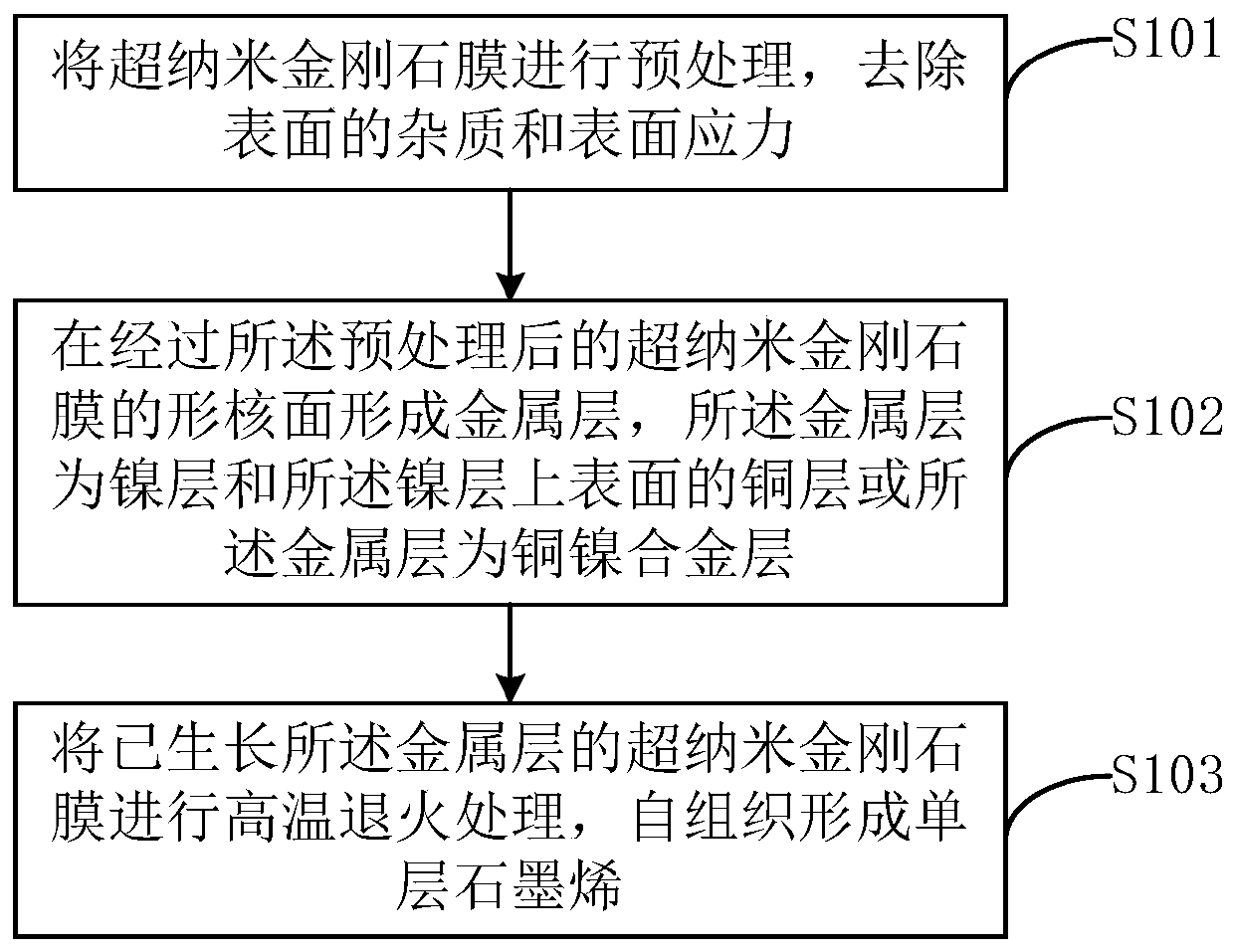
[0033] Please refer to figure 1 , the method for preparing single-layer graphene on the surface of the ultra-nanodiamond film comprises:
[0034] In step S101 , the ultra-nano-diamond film is pretreated to remove surface impurities and surface stress.
[0035] Optionally, the implementation of step S101 is:
[0036] Putting the ultra-nano-diamond film into a strong acid solution for the first cleaning;
[0037] The ultra-nano-diamond film is placed in acetone and alcohol solution in sequence for ultrasonic cleaning;
[0038] The ultra-nano-diamond film is subjected to microwave plasma treatment to fully remove the surface stress of the ultra-nano-diamond film.
[0039] In the embodiment of the present invention, the strong acid solution is a mixed solution of concentrated sulfuric acid and concentrated nitric acid with a volume ratio of 8:1. First, put the ultra-nano-diamond film into the mixed solution, and heat the temperature to 220°C for 30 minutes. Then, put the ultra...
Embodiment 2
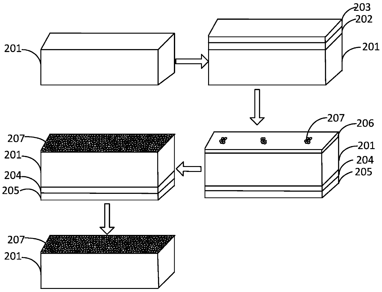
[0055] Please refer to figure 2 , the method for preparing single-layer graphene on the surface of ultra-nanometer diamond comprises the following steps:
[0056] (1) The double-sided polished ultra-nano-diamond film 201 prepared by the microwave plasma chemical vapor deposition method is put into a strong acid solution to fully react. The strong acid solution is a solution of concentrated sulfuric acid and concentrated nitric acid with a volume ratio of 8:1. During treatment, the solution temperature is heated to 200°C, and the treatment time is 30 minutes. Wherein, the thickness of the super nano-diamond film 201 is 500 nanometers.
[0057] (2) Place the ultranano-diamond film 201 in acetone and alcohol solutions in sequence for ultrasonic cleaning. Ultrasonic cleaning time of the ultranano-diamond film 201 in acetone and alcohol solutions is 30 minutes.
[0058] (3) The ultra-nanometer diamond film 201 is subjected to microwave hydrogen plasma treatment, the plasma powe...
Embodiment 3
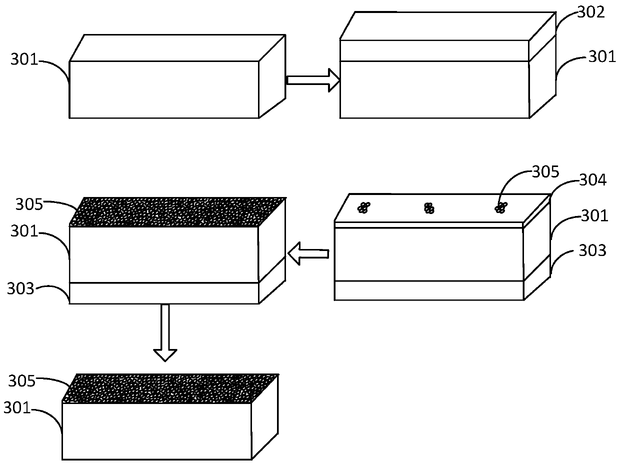
[0064] Please refer to image 3 , the method for preparing single-layer graphene on the surface of ultra-nanometer diamond comprises:
[0065] (1) The double-sided polished ultra-nano-diamond film 301 prepared by the microwave plasma chemical vapor deposition method is put into a strong acid solution to fully react. The strong acid solution is a solution of concentrated sulfuric acid and concentrated nitric acid with a volume ratio of 8:1. During treatment, the solution temperature is heated to 200°C, and the treatment time is 30 minutes. Wherein, the thickness of the super nano-diamond film 201 is 800 nanometers.
[0066] (2) The ultra-nano-diamond film 301 is sequentially placed in acetone and alcohol solutions for ultrasonic cleaning. Ultrasonic cleaning time of the ultranano-diamond film 301 in acetone and alcohol solutions is 30 minutes.
[0067] (3) The ultra-nano-diamond film 301 is subjected to microwave hydrogen plasma treatment, the plasma power is 3kW, and the tr...
PUM
| Property | Measurement | Unit |
|---|---|---|
| thickness | aaaaa | aaaaa |
| thickness | aaaaa | aaaaa |
| thickness | aaaaa | aaaaa |
Abstract
Description
Claims
Application Information