Method for preparing single-layer graphene on surface of ultranano diamond

A single-layer graphene and ultra-nano technology, applied in the direction of single-layer graphene, diamond, graphene, etc., can solve problems such as defects and impurity lattices, achieve small lattice mismatch and surface changes, promote nucleation, Avoid the effects of impurities and lattice defects

Active Publication Date: 2018-04-13
THE 13TH RES INST OF CHINA ELECTRONICS TECH GRP CORP
View PDF5 Cites 4 Cited by
  • Summary
  • Abstract
  • Description
  • Claims
  • Application Information

AI Technical Summary

Problems solved by technology

[0004] In view of this, the embodiment of the present invention provides a method for preparing single-layer graphene on the surface of ultra-nano diamond to solve the problem that the method for preparing graphene on the surface of diamond in the prior art will introduce impurities and lattice defects

Method used


Image

  • Method for preparing single-layer graphene on surface of ultranano diamond
  • Method for preparing single-layer graphene on surface of ultranano diamond
  • Method for preparing single-layer graphene on surface of ultranano diamond

Examples


Embodiment 1

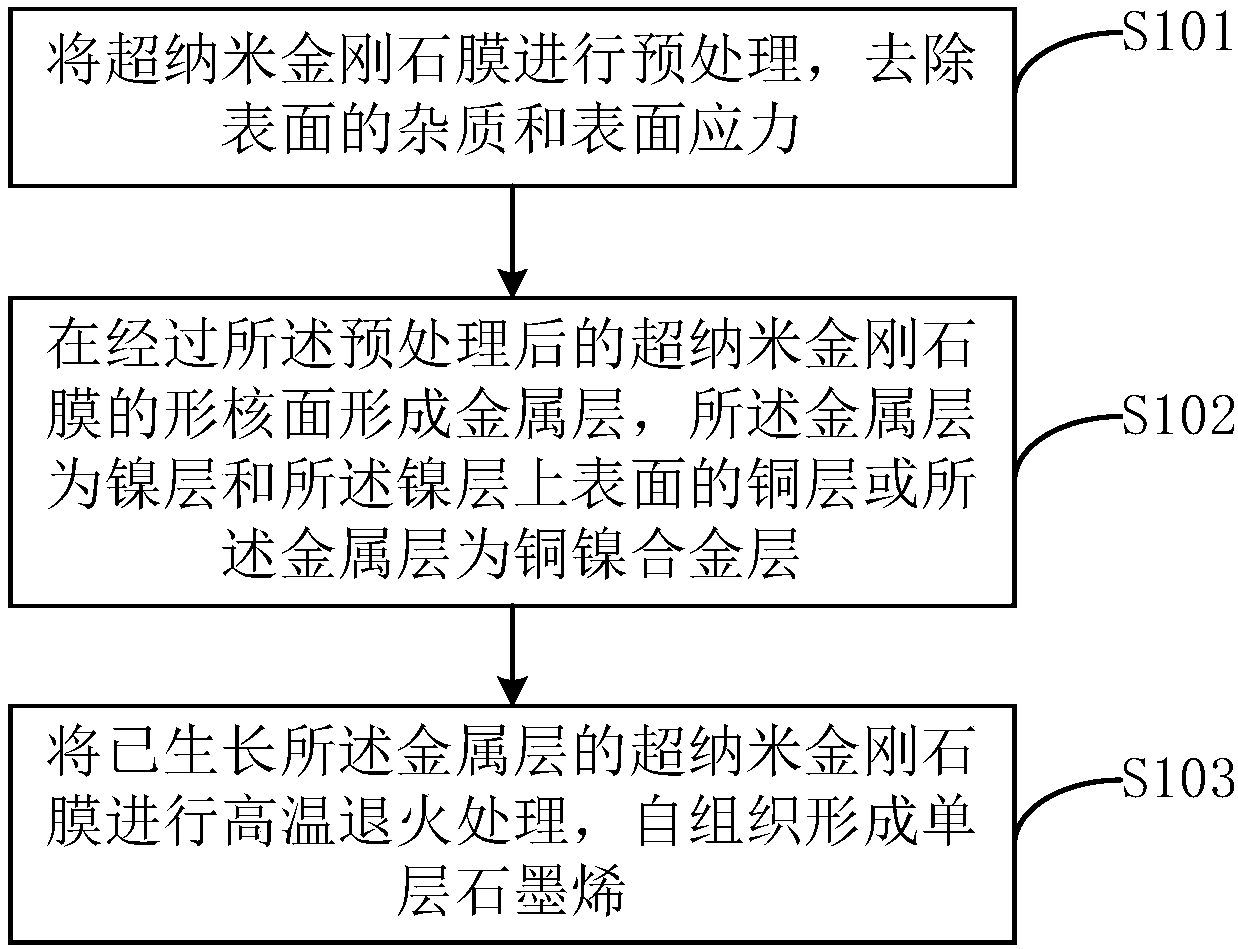
[0033] Please refer to figure 1 , the method for preparing single-layer graphene on the surface of the ultra-nanodiamond film comprises:

[0034] In step S101 , the ultra-nano-diamond film is pretreated to remove surface impurities and surface stress.

[0035] Optionally, the implementation of step S101 is:

[0036] Putting the ultra-nano-diamond film into a strong acid solution for the first cleaning;

[0037] The ultra-nano-diamond film is placed in acetone and alcohol solution in sequence for ultrasonic cleaning;

[0038] The ultra-nano-diamond film is subjected to microwave plasma treatment to fully remove the surface stress of the ultra-nano-diamond film.

[0039] In the embodiment of the present invention, the strong acid solution is a mixed solution of concentrated sulfuric acid and concentrated nitric acid with a volume ratio of 8:1. First, put the ultra-nano-diamond film into the mixed solution, and heat the temperature to 220°C for 30 minutes. Then, put the ultra...

Embodiment 2

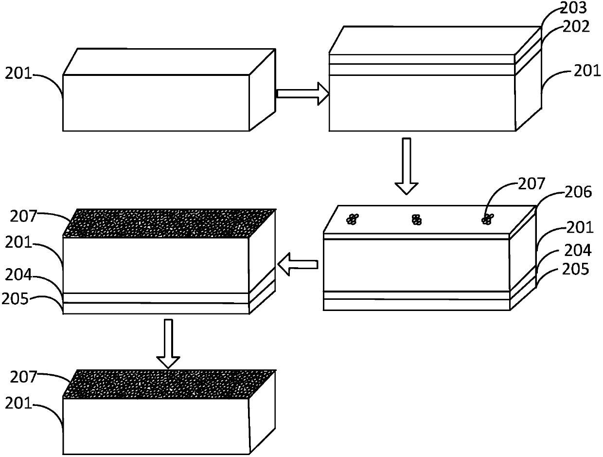
[0055] Please refer to figure 2 , the method for preparing single-layer graphene on the surface of ultra-nanometer diamond comprises the following steps:

[0056] (1) The double-sided polished ultra-nano-diamond film 201 prepared by the microwave plasma chemical vapor deposition method is put into a strong acid solution to fully react. The strong acid solution is a solution of concentrated sulfuric acid and concentrated nitric acid with a volume ratio of 8:1. During treatment, the solution temperature is heated to 200°C, and the treatment time is 30 minutes. Wherein, the thickness of the super nano-diamond film 201 is 500 nanometers.

[0057] (2) Place the ultranano-diamond film 201 in acetone and alcohol solutions in sequence for ultrasonic cleaning. Ultrasonic cleaning time of the ultranano-diamond film 201 in acetone and alcohol solutions is 30 minutes.

[0058] (3) The ultra-nanometer diamond film 201 is subjected to microwave hydrogen plasma treatment, the plasma powe...

Embodiment 3

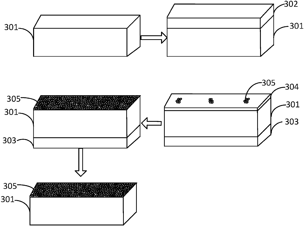
[0064] Please refer to image 3 , the method for preparing single-layer graphene on the surface of ultra-nanometer diamond comprises:

[0065] (1) The double-sided polished ultra-nano-diamond film 301 prepared by the microwave plasma chemical vapor deposition method is put into a strong acid solution to fully react. The strong acid solution is a solution of concentrated sulfuric acid and concentrated nitric acid with a volume ratio of 8:1. During treatment, the solution temperature is heated to 200°C, and the treatment time is 30 minutes. Wherein, the thickness of the super nano-diamond film 201 is 800 nanometers.

[0066] (2) The ultra-nano-diamond film 301 is sequentially placed in acetone and alcohol solutions for ultrasonic cleaning. Ultrasonic cleaning time of the ultranano-diamond film 301 in acetone and alcohol solutions is 30 minutes.

[0067] (3) The ultra-nano-diamond film 301 is subjected to microwave hydrogen plasma treatment, the plasma power is 3kW, and the tr...


PUM

PropertyMeasurementUnit
thicknessaaaaaaaaaa
thicknessaaaaaaaaaa
thicknessaaaaaaaaaa

Abstract

The invention is applicable to the technical field of semiconductor and provides a method for preparing single-layer graphene on the surface of ultranano diamond. The method comprises preprocessing anultranano diamond film to eliminate surface impurities and surface stress; forming a metal layer on the nucleation surface of the preprocessed ultranano diamond film, wherein the metal layer is composed of a nickel layer and a copper layer on the upper surface of the nickel layer or is a copper-nickel alloy layer; performing high-temperature annealing treatment on the ultranano diamond film withthe grown metal layer to self-organize the single-layer graphene. The method for preparing the single-layer graphene on the surface of the ultranano diamond saves a second transfer process by directlygrowing the single-layer graphene on the ultranano diamond film, thereby effectively avoiding introduced impurities and lattice imperfection during second transfer processes; meanwhile, the grown single-layer graphene is small in lattice mismatch and surface change.

Description

technical field [0001] The invention belongs to the technical field of semiconductors, in particular to a method for preparing single-layer graphene on the surface of ultranano diamond. Background technique [0002] Graphene has outstanding physical, mechanical, chemical, and electrical properties, and has important potential applications in the fields of high-frequency electronic devices, optoelectronic devices, and high-sensitivity sensors. Diamond has excellent properties such as extremely high hardness and thermal conductivity, excellent thermal shock resistance, and chemical stability. As a graphene matrix material, diamond has unique properties compared with traditional insulating materials such as metals, silicon dioxide, and silicon carbide. Advantage. The energy band structure of single-layer graphene presents a standard Dirac cone, which has unique advantages over multi-layer graphene. The direct preparation of single-layer graphene on the diamond surface can eff...

Claims


Application Information

Patent Timeline
Patent Type & Authority Applications(China)
IPC IPC(8): C01B32/28C01B32/184
CPCC01B2204/02
Inventor 郭建超蔚翠冯志红房玉龙何泽召王晶晶刘庆彬周闯杰高学栋
Owner THE 13TH RES INST OF CHINA ELECTRONICS TECH GRP CORP
Why Eureka
Try Eureka