Light-emitting device, illuminating apparatus, and display apparatus

a technology of light-emitting devices and illuminating devices, which is applied in the direction of semiconductor devices for light sources, lighting and heating devices, instruments, etc., can solve the problems of inability to accurately align with each other, increase the size of the bezel portion of the display panel, and the use of backlight units that are not suitable for backlighting, etc., to achieve efficient diffusion of light incident, high accuracy, and high accuracy

Inactive Publication Date: 2014-12-25
SHARP KK
View PDF12 Cites 30 Cited by
  • Summary
  • Abstract
  • Description
  • Claims
  • Application Information

AI Technical Summary

Benefits of technology

[0039]According to the invention, the light-emitting device comprises the light-emitting element that emits light, the base support that supports the light-emitting element, and the columnar optical member disposed on the light-emitting surface side of the light-emitting element so as to cover the light-emitting element in contact therewith, the columnar optical member reflecting or refracting light in a plurality of directions. The optical member has a top surface which faces the illumination object and is shaped so as to have a recess at a center thereof. The top surface of the optical member includes the first region which reflects light emitted from the light-emitting element and travels in the interior of the optical member so that the light exits from the side surface of the optical member to the outside, and the second region which refracts light traveling in the interior so that the light exits from the top surface, wherefore light incident on the optical member can be diffused by the top surface. Moreover, in the light-emitting device of the invention, the optical member is placed in contact with the light-emitting element, wherefore the optical member and the light-emitting element are disposed in a highly accurate alignment with each other. This allows the light-emitting device to reflect and refract light emitted from the light-emitting element with high accuracy by the action of the optical member kept in contact with the light-emitting element, and accordingly, the light-emitting device is, even when used in a low-profile display apparatus, capable of applying light to the illumination object with uniformity in brightness in the planar direction.
[0040]It is noted that light is emitted from the light-emitting element in a radial fashion about the optical axis. In view of this radial emission of light from the light-emitting element, for the sake of uniformity in brightness in the planar direction of the illumination object, the optical member is configured to have the first region having a light-reflecting capability and the second region having a light-refracting capability.
[0041]Moreover, according to the invention, the first region lies closer to the light-emitting element than the second region. This makes it possible to achieve efficient diffusion of light incident on the optical member.
[0042]In general, light from a LED, which is a light-emitting element that emits light, peaks in intensity around the optical axis, and decreases in intensity as it travels outward from the optical axis. Accordingly, in order to apply light to a place located far away from the light-emitting element with high efficiency, it is necessary to effect irradiation with light of even higher intensity, and thus, uniformity in light intensity in the device as a whole is attained by applying near-optical-axis light to a distant place, whereas using low-intensity light away from the optical axis for a place close to the light-emitting element where an extra light intensity is not so required.
[0043]In the invention, to ensure that the distant place is irradiated with light around the optical axis of the light-emitting element, the optical member has the first region in the vicinity of the optical axis, and the second region located externally circumferentially of the first region.
[0044]Moreover, according to the invention, the light quantity attenuation portion is disposed in the recess located at the center of the top surface of the optical member, the light quantity attenuation portion diminishing the quantity of incident light. By virtue of the light quantity attenuation portion, it is possible to achieve reduction in the quantity of light emitted from the central recess of the top surface of the optical member specifically for a region directly above the light-emitting element where a large quantity of light reaches. Accordingly, the light-emitting device is capable of preventing localized brightness variations in the planar direction of the illumination object.

Problems solved by technology

Although the LED has excellent characteristics, including lower power consumption, longer service life, and the capability of reduction in environmental burdens without the use of mercury, its use as a light source for a backlight unit has fallen behind because of its expensiveness, the fact that there had been no white-color LED prior to the invention of a blue-color LED, and its high directivity.
However, the edge-lighting type backlight unit poses the following problems: localized arrangement of light sources at the edge portion of the light guide plate results in concentration of heat generated by the light sources; and the size of the bezel portion of the display panel is inevitably increased.
Furthermore, the edge-lighting type backlight unit is subjected to severe restrictions in terms of local dimming control which attracts attention as a control technique capable of display of high-quality images and energy saving, and is therefore incapable of split-region control that achieves production of high-quality displayed images and low power consumption as well.

Method used


Image

  • Light-emitting device, illuminating apparatus,  and display  apparatus
  • Light-emitting device, illuminating apparatus,  and display  apparatus
  • Light-emitting device, illuminating apparatus,  and display  apparatus

Examples


Embodiment Construction

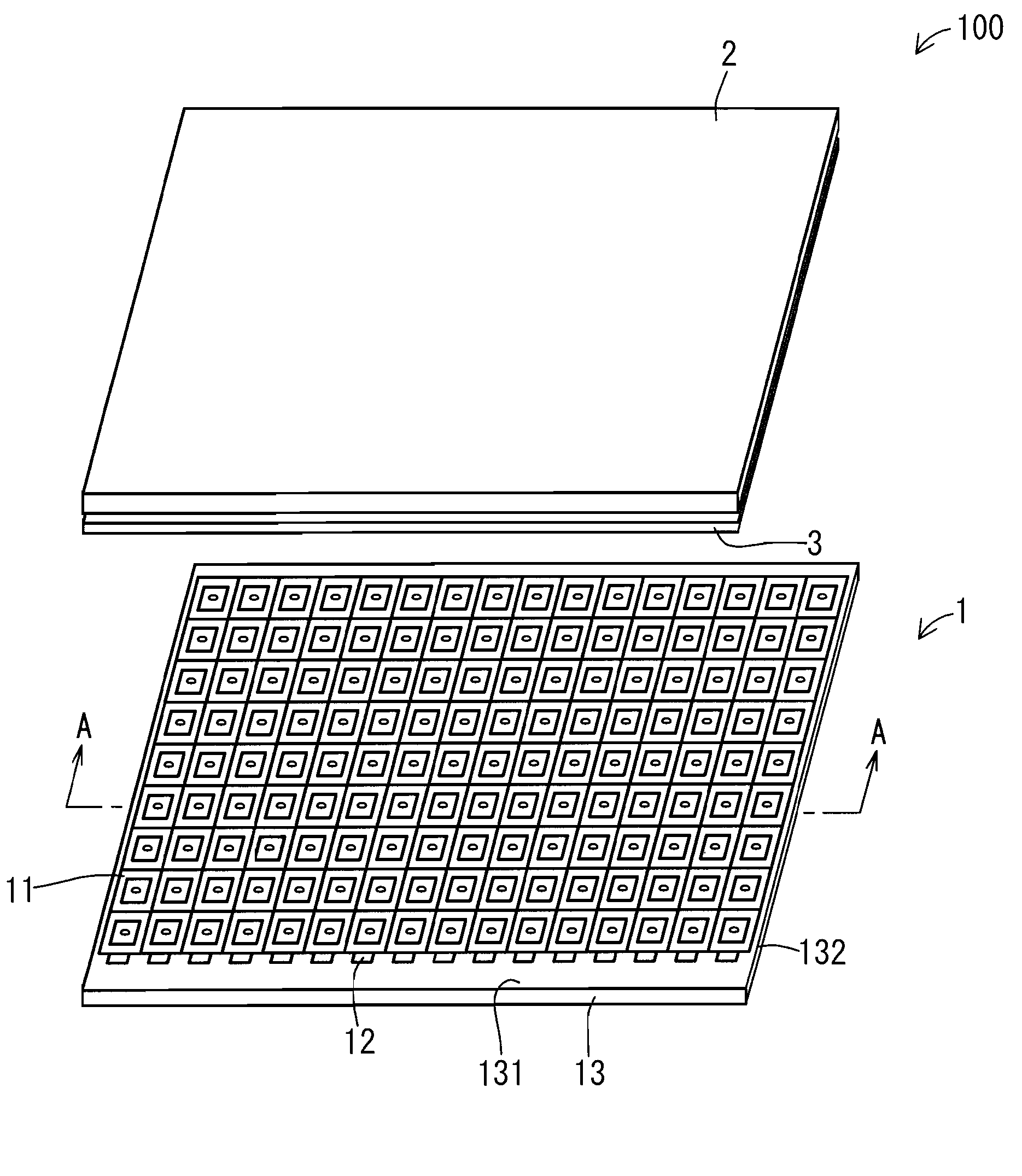
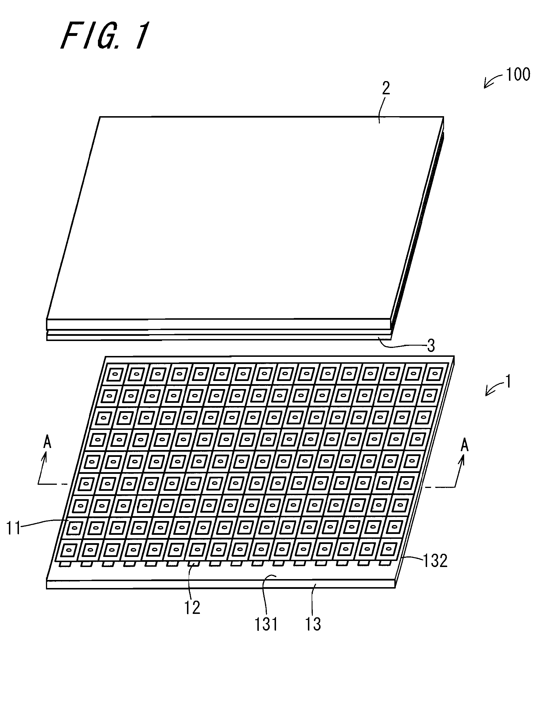
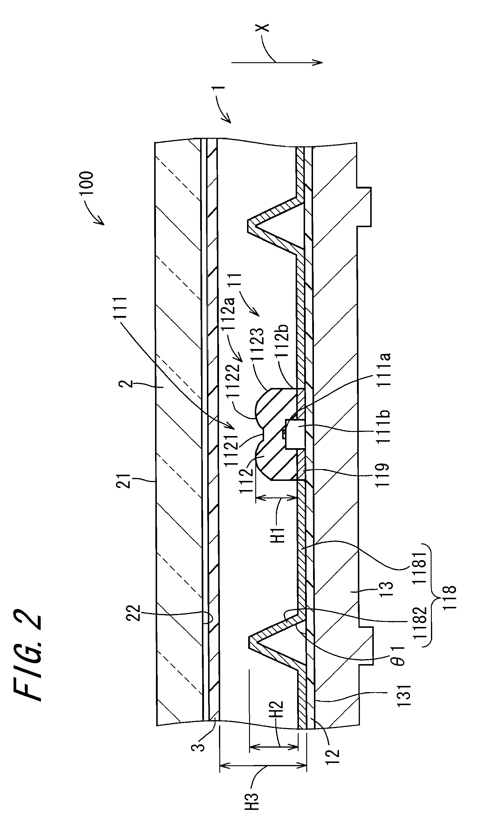
[0090]FIG. 1 is an exploded perspective view showing the structure of a liquid-crystal display apparatus 100 in accordance with a first embodiment of the invention. FIG. 2 is a sectional view of the liquid-crystal display apparatus 100 taken along the line A-A of FIG. 1. FIG. 3 is a view showing a state where a plurality of light-emitting devices 11 are arranged in an orderly manner. The liquid-crystal display apparatus 100 which is a display apparatus according to the invention is designed for use in television sets, personal computers, and so forth, for showing an image on a display screen in response to output of image information. The display screen is constructed of a liquid-crystal panel 2 which is a transmissive display panel having liquid-crystal elements, and the liquid-crystal panel 2 has the form of a rectangular flat plate. In the liquid-crystal panel 2, two sides in a thickness-wise direction thereof will be referred to as a front 21 side and a back 22 side, respectivel...


PUM


Abstract

The invention provides a light-emitting device which is capable of applying light to a display panel with uniformity in brightness and can be made lower in profile. A light-emitting device (11) includes an LED chip (111a), a base support (111b) which supports the LED chip (111a), and a lens (112) disposed in contact with the LED chip (111a) so as to cover the LED chip (111a) and the base support (111b). The lens (112) has first curved sections (1122) which reflect light that has reached a top surface (112a) so that the reflected light is emitted from a side surface (112b), and second curved sections (1123) which refract light that has reached the top surface (112a) to outside so that the refracted light is emitted from the top surface (112a).

Description

TECHNICAL FIELD[0001]The present invention relates to a light-emitting device which is disposed in a backlight unit for applying light to a display panel from a back side, and an illuminating apparatus and a display apparatus including the light-emitting device.BACKGROUND ART[0002]In a display panel in which a liquid crystal is sealed in between two transparent substrates, upon application of voltage, the orientations of liquid crystal molecules are changed with consequent variations in light transmittance, so that a predetermined image or the like is displayed in an optical manner. In the display panel, since the liquid crystal does not emit light by itself as a light emitter, for example, a transmissive liquid crystal panel has, at its back side, a backlight unit for effecting irradiation of light from a light source such as a cold-cathode tube (CCFL) or a light-emitting diode (LED).[0003]Backlight units are classified into two categories, namely a direct-lighting type in which li...

Claims


Application Information

Patent Timeline
Patent Type & Authority Applications(United States)
IPC IPC(8): F21V7/00F21V5/00
CPCF21V5/00F21V7/0025G02F1/1303G02F1/133603G02F1/133605H01L33/54B29D11/00807H01L2224/73265H01L25/0753H01L2933/005G02F1/133606G02F1/133613G02F1/133607F21K9/68F21V5/045
Inventor ONO, YASUHIROMASUDA, MAKOTOWADA, TAKASUMIOHKUBO, KENZOSHIRAI, NOBUHIRO
Owner SHARP KK
Why Eureka
Try Eureka