Optical semiconductor device and method of manufacturing same

a technology of optical semiconductor and manufacturing method, which is applied in the direction of semiconductor lasers, instruments, optical elements, etc., can solve the problems of difficult to deal with situations, optical transmission efficiency and yield, and achieve the effect of high precision alignmen

Inactive Publication Date: 2005-03-31
NEC ELECTRONICS CORP
View PDF12 Cites 12 Cited by
  • Summary
  • Abstract
  • Description
  • Claims
  • Application Information

AI Technical Summary

Benefits of technology

[0016] Accordingly, an object of the present invention is to provide an optical semiconductor device and a method of manufacturing the same, in which optical parts, particularly a semiconductor light-source chip and an optical lens, can be mutually aligned with high accuracy by simple working of the substrate on which the optical parts are mounted, without using a mounting apparatus having high alignment accuracy.
[0039] In this case, by forming the guide grooves of the aforesaid shape by etching the substrate chemically, physically or chemically and physically, the guide grooves having the aforesaid shape can be formed in highly accurate fashion by simple working of the substrate on which the optical parts are mounted. As a result, by merely accommodating the optical parts, particularly a semiconductor light-source chip having the shape of a rectangular parallelepiped and an optical lens member having the shape of a rectangular parallelepiped, in the guide grooves and bringing them into abutting contact with side surfaces of the guide grooves, the optical axes of the semiconductor light-source chip and optical lens can be brought into highly precise alignment without using a mounting apparatus having a high alignment accuracy.

Problems solved by technology

However, nowhere do these references describe adjustment of the optical axes between these parts in a case where an optical lens is interposed between them.
Since this necessitates highly sophisticated mold or cutting technology, it will be difficult to deal with situations in the future where an improvement in optical transmission efficiency and yield are required.

Method used


Image

  • Optical semiconductor device and method of manufacturing same
  • Optical semiconductor device and method of manufacturing same
  • Optical semiconductor device and method of manufacturing same

Examples


first embodiment

[0048] [First Embodiment]

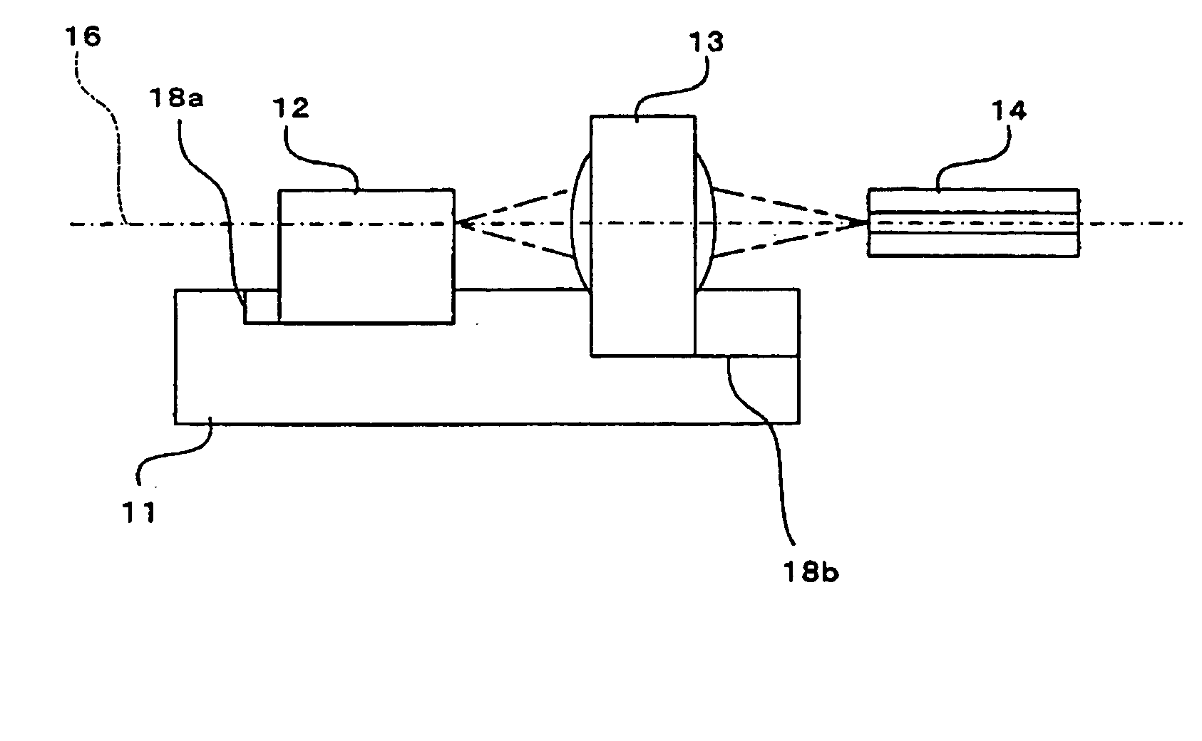
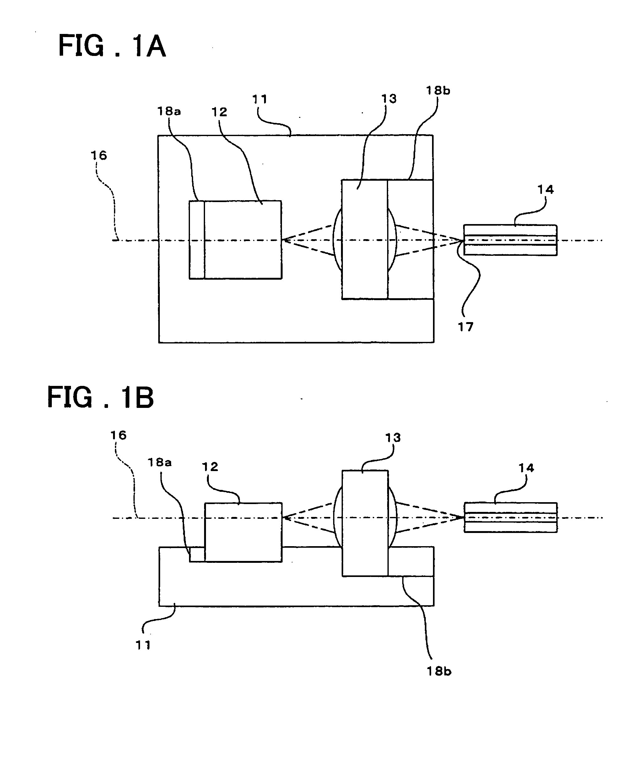
[0049]FIGS. 1A and 1B are diagrams illustrating the structure of an optical semiconductor device according to a first embodiment of the present invention, in which FIG. 1A is a plan view and FIG. 1B a sectional view taken along an optical axis 16 in FIG. 1A.

[0050] As shown in FIGS. 1A and 1B, the optical semiconductor device comprises a substrate 11 and a plurality of optical parts.

[0051] A silicon substrate having a surface with (110) surface orientation is used as the substrate 11, and a semiconductor laser chip (semiconductor light-source chip) 12 having the shape of a rectangular parallelepiped, an optical lens member 13 having the shape of a rectangular parallelepiped and an optical fiber 14 are provided as the optical parts. These optical parts are aligned with one another in terms of the optical axis 16 and are optically coupled.

[0052] Among these optical parts, the semiconductor laser chip 12 and optical lens member 13 are mounted on the substrate...

second embodiment

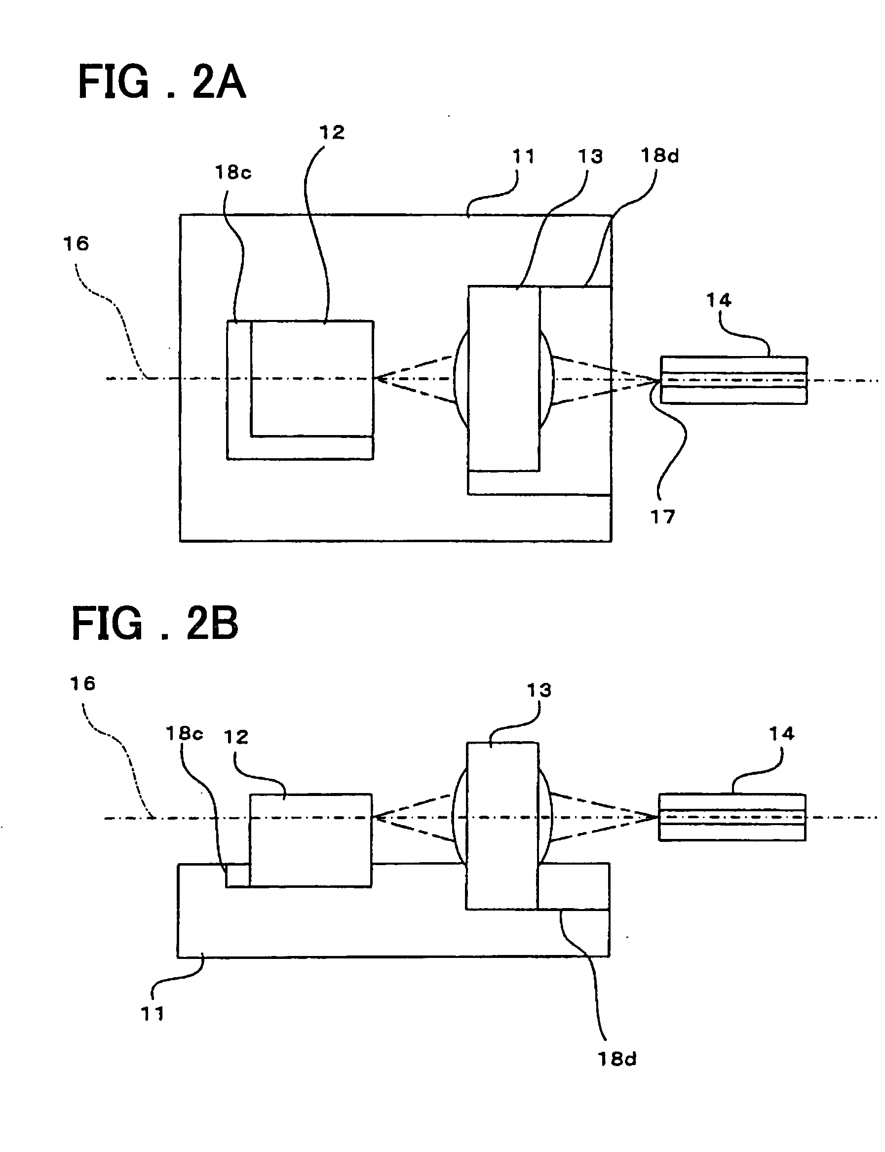
[0062] [Second Embodiment]

[0063] A method of manufacturing the above-described optical semiconductor device according to a second embodiment of the present invention will now be described.

[0064] First, a silicon substrate having a surface with (110) surface orientation is prepared as the substrate 11. Next, the guide grooves 18a, 18b for accommodating the semiconductor laser chip 12 and optical lens member 13 each having the shape of a rectangular parallelepiped, respectively, are formed in the substrate 11 at the mounting positions of these optical parts.

[0065] The guide grooves 18a, 18b formed each have first side surfaces orthogonal to the direction of the optical axis 16, second side surfaces parallel to the direction of the optical axis 16 and substantially perpendicular to the surface of the substrate 11, and a bottom surface substantially parallel to the surface of the substrate 11. Each guide groove has a size and a depth that allow at least a bottom portion of the corresp...


PUM


Abstract

An optical semiconductor device includes a substrate and a plurality of optical parts mounted thereon. Guide grooves are formed in the substrate at the mounting positions of the optical parts. Each guide groove has first side surfaces, which are substantially orthogonal to the direction of the optical axis, second side surfaces, which are substantially parallel to the direction of the optical axis and substantially perpendicular to the surface of the substrate, and a bottom surface substantially parallel to the surface of the substrate. Each guide groove has a size and a depth that allow at least a bottom portion of the corresponding optical part to be received therein. The corresponding optical part is accommodated in each guide groove in abutting contact with the first side surfaces of the guide groove, whereby the optical parts are aligned with one another along the direction of the optical axis.

Description

FIELD OF THE INVENTION [0001] This invention relates to an optical semiconductor device and method of manufacturing the same. More particularly, the invention relates to an optical semiconductor device in which a plurality of optical parts are mounted on a substrate and optically coupled, and to a method of manufacturing this device. BACKGROUND OF THE INVENTION [0002] An optical semiconductor device of the kind shown in FIGS. 3A and 3B is an example of an optical semiconductor device according to the prior art. FIG. 3A is a plan view illustrating this optical semiconductor device according to the prior art, and FIG. 3B is a sectional view taken along optical axis 6 in FIG. 3A. [0003] This optical semiconductor device includes a substrate 1 and a semiconductor laser chip 2, optical lens 3 and optical fiber 4 placed on the substrate 1 along the optical axis 6 in the order mentioned starting from the side of the semiconductor laser chip 2. These optical parts are aligned with one anoth...

Claims


Application Information

Patent Timeline
Patent Type & Authority Applications(United States)
IPC IPC(8): H01S5/022G02B6/26G02B6/42
CPCG02B6/423G02B6/4204
Inventor ARAYAMA, TATSURO
Owner NEC ELECTRONICS CORP
Why Eureka
Try Eureka