Array substrate and manufacturing method thereof, and display screen

The technology of an array substrate and its manufacturing method is applied in the fields of the array substrate and its manufacturing method and the display screen, which can solve problems such as poor screen body and easy breakage, and achieve the effects of preventing breakage, prolonging the service life, and ensuring the transmission of signals

Active Publication Date: 2018-04-13
KUNSHAN GO VISIONOX OPTO ELECTRONICS CO LTD
View PDF6 Cites 26 Cited by
  • Summary
  • Abstract
  • Description
  • Claims
  • Application Information

AI Technical Summary

Problems solved by technology

[0003] However, in the current display screen, during the bending process of the non-display area, the

Method used


Image

  • Array substrate and manufacturing method thereof, and display screen
  • Array substrate and manufacturing method thereof, and display screen
  • Array substrate and manufacturing method thereof, and display screen

Examples


Embodiment Construction

[0032] In order to make the object, technical solution and advantages of the present invention clearer, the present invention will be further described in detail below in conjunction with the accompanying drawings and embodiments. It should be understood that the specific embodiments described here are only used to explain the present invention, not to limit the present invention.

[0033] It should be noted that when an element is referred to as being “disposed on” another element, it may be directly on the other element or there may also be an intervening element. When an element is referred to as being "connected to" another element, it can be directly connected to the other element or intervening elements may also be present. The terms "vertical," "horizontal," "left," "right," and similar expressions are used herein for purposes of illustration only and are not intended to represent the only embodiments.

[0034] Unless otherwise defined, all technical and scientific ter...


PUM


Abstract

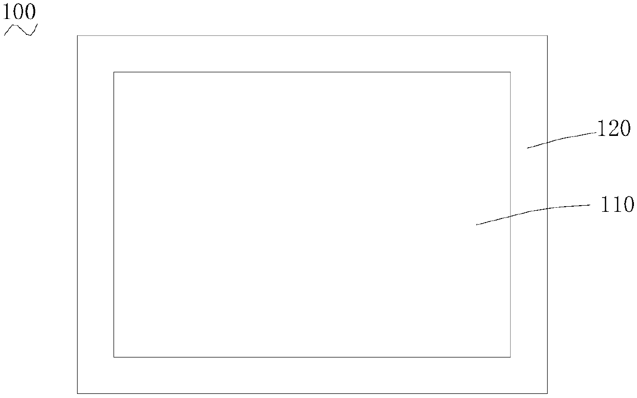
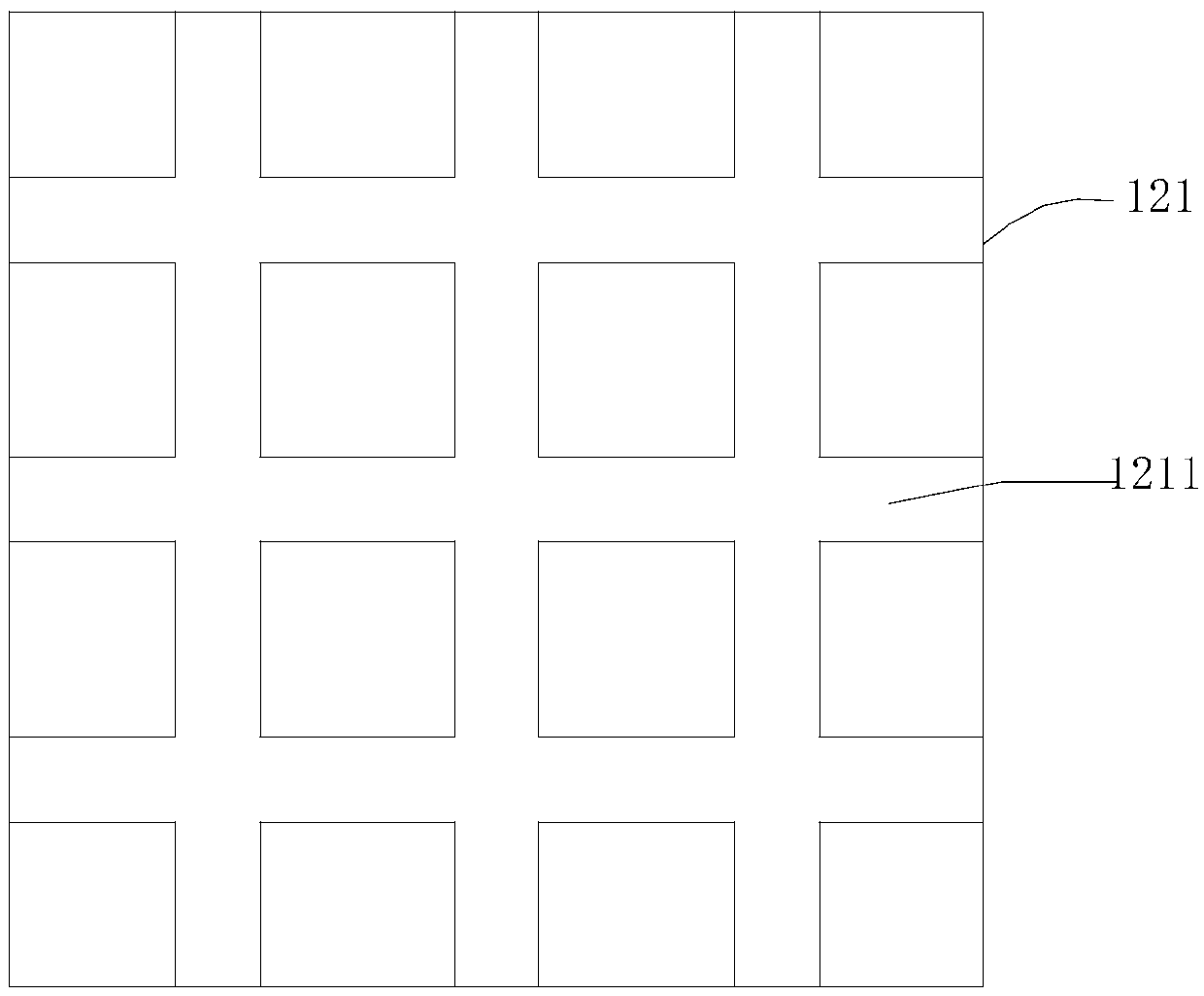
The invention relates to an array substrate. The array substrate comprises a display region and a non-display region positioned on the outer side of the display region; and the non-display region comprises a flexible substrate with multiple grooves in the surface, and peripheral metal lines positioned in the grooves. According to the array substrate, the grooves are formed in the surface of the substrate, and the peripheral metal lines are positioned in the grooves, so that the thickness, in the peripheral metal lines, of the flexible substrate is reduced, and extrusion of the flexible substrate on the peripheral metal lines is reduced in a bending process; and in addition, by virtue of setting of the grooves, the stress of the flexible substrate can be effectively released in bending, thereby effectively preventing cracking of the peripheral metal lines and improving reliability of the array substrate. The invention also provides a display screen and a manufacturing method of the array substrate.

Description

technical field [0001] The invention relates to the field of display technology, in particular to an array substrate, a manufacturing method thereof, and a display screen. Background technique [0002] The display screen includes a display area (AA area) and a non-display area (non-AA area). In order to achieve certain functions, the non-display area is required to be bendable. For example, in order to achieve a narrow frame, the non-display area is bent to the back of the screen, thereby reducing the width of the frame. [0003] However, in the current display screen, during the bending process of the non-display area, the peripheral metal wires in the non-display area are easily broken, thus causing a defective screen body. Contents of the invention [0004] Based on this, it is necessary to provide an array substrate that can effectively prevent the peripheral metal wires from breaking. [0005] An array substrate, including a display area, and a non-display area loca...

Claims


Application Information

Patent Timeline
IPC IPC(8): H01L27/12H01L21/84
CPCH01L27/1244H01L27/1259H01L27/1218H01L27/1262H01L27/127
Inventor 刘明星张德强吕东芸王徐亮甘帅燕高峰
Owner KUNSHAN GO VISIONOX OPTO ELECTRONICS CO LTD
Why Eureka
Try Eureka