Positioning base plate for PCB pore forming and positioning method thereof

A technology of PCB circuit board and positioning bottom plate, which is applied in the direction of printed circuit, printed circuit manufacturing, electrical components, etc., can solve the problems of increased product manufacturing cost, expensive positioning bottom plate, wrong positioning holes, etc., so as to avoid product waste and reduce Manufacturing cost, the effect of avoiding positioning errors

Active Publication Date: 2018-05-08
DALIAN CHONGDA CIRCUIT
View PDF4 Cites 1 Cited by
  • Summary
  • Abstract
  • Description
  • Claims
  • Application Information

AI Technical Summary

Problems solved by technology

[0003] like figure 1 As shown, when using this method to process, before each type of product is processed, the matching positioning holes 01 must be processed on the bottom plate first. Over time, the positioning holes 01 of the positioning bottom plate will become very dense. The situation is very easy to cause the positioning holes to be used wrongly and the product will be discarded. Even if the base plate is replaced with a new one, it will soon become this state, and the price of this positioning base plate is relatively expensive, and frequent replacement will increase the manufacturing cost of the product. This state is a common phenomenon in all printed circuit board industries at present. This problem has plagued engineers and technicians for a long time, and there has been no fundamental and effective way to improve it.

Method used


Image

  • Positioning base plate for PCB pore forming and positioning method thereof
  • Positioning base plate for PCB pore forming and positioning method thereof
  • Positioning base plate for PCB pore forming and positioning method thereof

Examples


Embodiment Construction

[0031] The specific embodiment of the present invention will be further described in detail below in conjunction with the accompanying drawings.

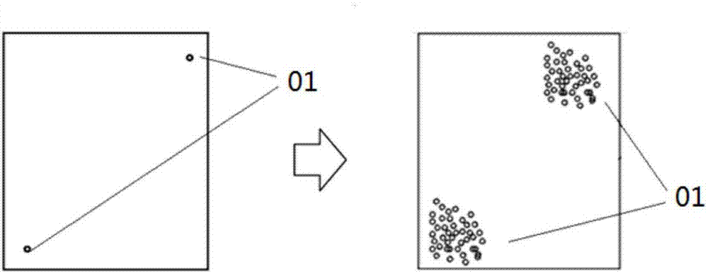
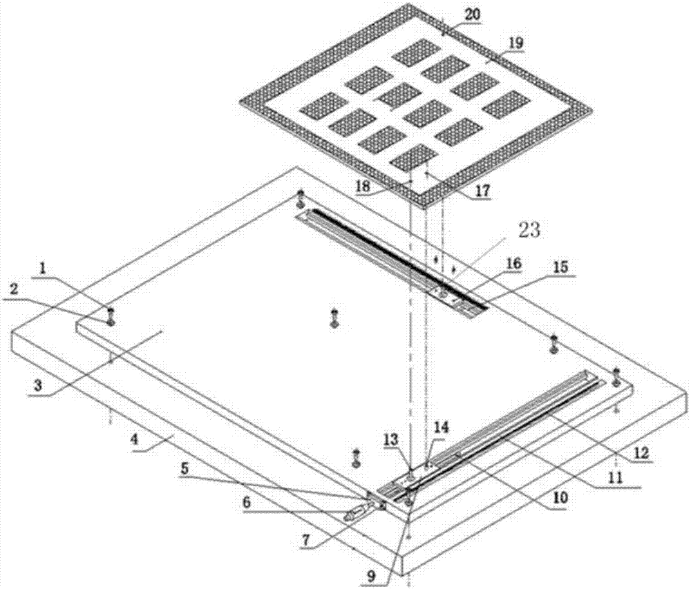
[0032] figure 2 It is a schematic diagram of a positioning base plate for forming a hole in a PCB circuit board of the present invention. The positioning base plate 3 for forming a hole in a PCB circuit board of the present invention is inserted into the positioning hole 2 of the base plate through the base plate positioning bolt 1 and fixed on the numerically controlled machine tool 4 when in use, as a hole to be processed. The carrier board of the PCB circuit board 17.

[0033] The two adjacent vertical sides of the positioning base plate 3 are respectively defined as a horizontal side in the X direction and a vertical side in the Y direction, and a horizontal side in the X direction and a vertical side in the Y direction are respectively provided with a side along the X direction and a side along the Y direction. The X-directio...


PUM


Abstract

The present invention discloses a positioning base plate for PCB pore forming and a positioning method thereof. Two mutually vertical slideways are processed in a positioning base plate, adjustable slide block sets capable of moving are arranged in the slideways, and a micrometer and a transmission screw are employed to perform accurate positioning of the adjustable slide block sets to achieve positioning of the PCB to be processed by employing stop bolts fixed at the upper surfaces of adjustable slide blocks. After the pore-forming processing operation of an No.1 PCB is completed, the positions of the adjustable slide blocks can be adjusted again to conveniently perform pore-forming processing of other types of PCBs, and therefore, the positioning base plate for PCB pore forming and the positioning method thereof have substantial characteristics such as one board with multiple functions, one board with common usage, avoiding of positioning errors and reduction of the manufacturing cost.

Description

technical field [0001] The invention belongs to the field of printed circuit board manufacturing, in particular to a positioning bottom plate for forming holes in a PCB circuit board and a positioning method. Background technique [0002] When the PCB circuit board is processed into holes, the positioning method of 1 side 2 holes or 1 side 3 holes is usually used to position the PCB circuit board to be processed on the positioning base plate, and the positioning method of 1 side 3 holes Among them, 1 hole is a process hole used to prevent reverse board. Therefore, when actually drilling, first install a special positioning base plate on the CNC machine table of the printed circuit board, and process 2 positioning holes on the base plate, such as figure 1 As shown in , the position of the positioning hole matches the size of the PCB circuit board to be processed, and then the positioning pin is installed in the positioning hole. The positioning hole and the positioning pin a...

Claims


Application Information

Patent Timeline
Patent Type & Authority Applications(China)
IPC IPC(8): H05K3/00
CPCH05K3/0044H05K2203/166H05K2203/167
Inventor 纪龙江
Owner DALIAN CHONGDA CIRCUIT
Why Eureka
Try Eureka