
A coupler and optical module

A technology of optical coupling and coupling area, applied in the field of optical communication applications, can solve the problems of low optical coupling efficiency of semiconductor lasers and silicon optical chips, etc.

Active Publication Date: 2020-09-11
HISENSE BROADBAND MULTIMEDIA TECH
View PDF4 Cites 0 Cited by
  • Summary
  • Abstract
  • Description
  • Claims
  • Application Information

AI Technical Summary

Problems solved by technology

[0006] In order to solve the technical problem of low optical coupling efficiency of semiconductor lasers and silicon optical chips in the related art, the present disclosure provides a coupler and an optical module

Method used


Image

  • A coupler and optical module
  • A coupler and optical module
  • A coupler and optical module

Examples


Embodiment Construction

[0036] Reference will now be made in detail to exemplary embodiments, examples of which are illustrated in the accompanying drawings. When the following description refers to the accompanying drawings, the same numerals in different drawings refer to the same or similar elements unless otherwise indicated. The implementations described in the following exemplary examples do not represent all implementations consistent with the present invention. Rather, they are merely examples of apparatuses and methods consistent with aspects of the invention as recited in the appended claims.

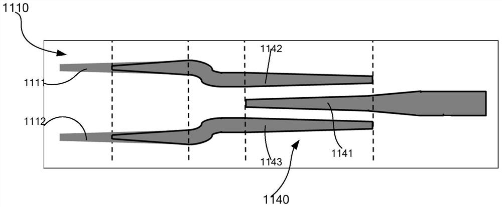
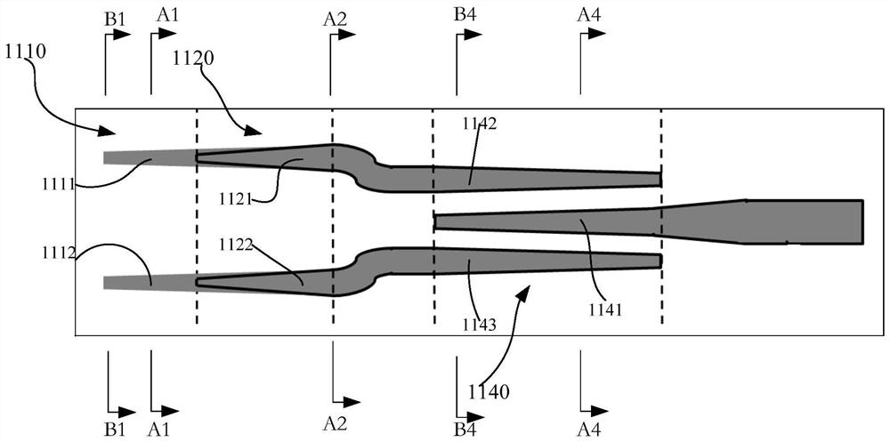
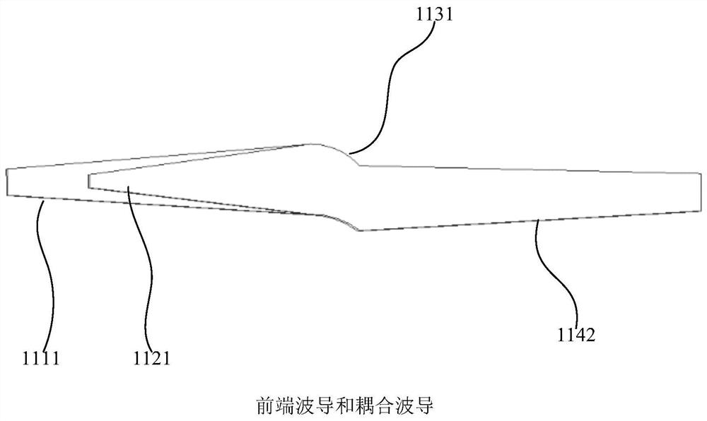
[0037] Such as figure 1 As shown, the present invention provides a coupler 1100 . figure 1 is a schematic structural diagram of the coupler 1100, Figure 7-17 It is a schematic cross-sectional view of different regions of the coupler 1100 in the length direction and a spot diagram formed by the cross-section of light passing through different regions.

[0038] Such as figure 1 As shown, the coup...


PUM


Abstract

The invention discloses a coupler and an optical module. The coupler is composed of a plurality of waveguides with gradually changing width and height. Along the length direction of the optical coupler, the front coupling area and the optical coupling area are sequentially arranged. Since the width and thickness of the front-end waveguide in the front-end coupling region are the smallest at the light-incident end, the optical coupler has multiple waveguide tips, and the mode spots of the multiple waveguide tips overlap each other, which can realize the matching between the optical coupler mode spot and the laser output mode spot. Matching, the light output by the laser is coupled into the silicon optical chip. The coupler has the advantages of simple structure and high optical coupling efficiency.

Description

technical field [0001] The present disclosure relates to the technical field of optical communication applications, in particular to a coupler and an optical module. Background technique [0002] With the increasingly higher bandwidth requirements for information transmission, the optical communication market has an increasing demand for high-speed optical modules above 100Gbps. It has become an urgent need to develop high-bandwidth, low-cost and high-integration high-speed optical modules using silicon photonics integration technology. [0003] At present, passive silicon optical devices such as high-speed silicon optical modulators, high-speed detectors, low-loss transmission waveguides, and wavelength division multiplexing have been fabricated on silicon optical chips. And it realizes single-channel 25Gpbs or 50Gbps information transmission by integrating various functional devices on the same silicon photonics chip. [0004] However, silicon is an indirect bandgap mate...

Claims


Application Information

Patent Timeline
Patent Type & Authority Patents(China)
IPC IPC(8): G02B6/42
CPCG02B6/4206G02B6/4291
Inventor 隋少帅
Owner HISENSE BROADBAND MULTIMEDIA TECH
Learn More