Array substrate, manufacturing method thereof, display panel and display device

A technology for array substrates and base substrates, applied in the fields of array substrates, manufacturing methods, display panels, and display devices, can solve the problems of low fingerprint recognition speed and sensitivity, and achieve improved speed and sensitivity, fast response speed, and small size Effect

Active Publication Date: 2022-06-21
BOE TECH GRP CO LTD
View PDF0 Cites 0 Cited by
  • Summary
  • Abstract
  • Description
  • Claims
  • Application Information

AI Technical Summary

Problems solved by technology

However, using photosensitive diodes as photosensitive elements, the speed and sensitivity of fingerprint recognition are not high.

Method used


Image

  • Array substrate, manufacturing method thereof, display panel and display device
  • Array substrate, manufacturing method thereof, display panel and display device
  • Array substrate, manufacturing method thereof, display panel and display device

Examples


Embodiment Construction

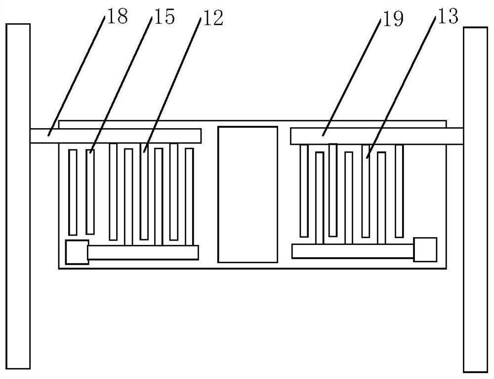
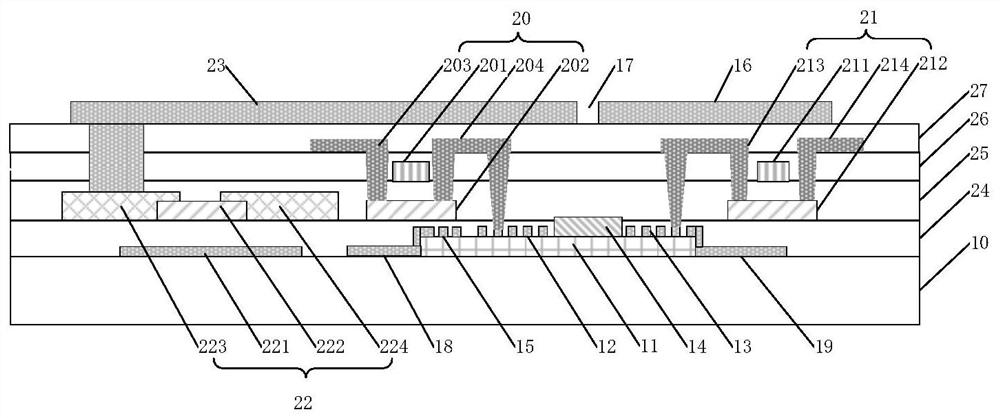
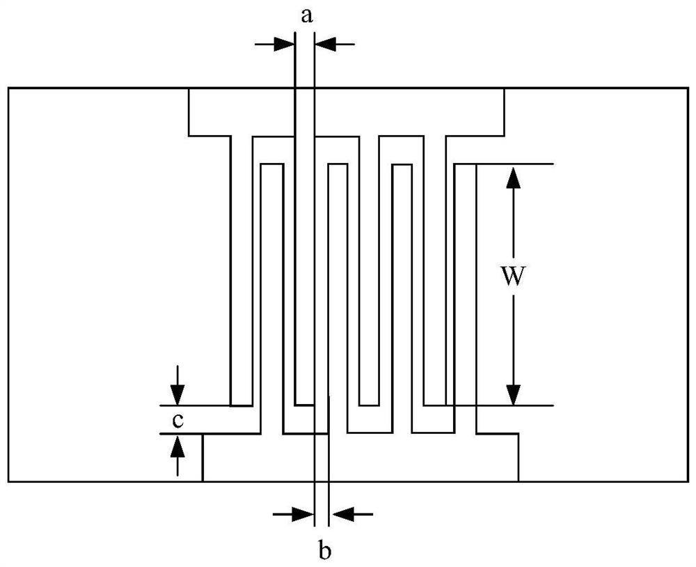
[0046] In order to illustrate the present invention more clearly, the present invention will be further described below with reference to the preferred embodiments and accompanying drawings. Similar parts in the figures are denoted by the same reference numerals. Those skilled in the art should understand that the content specifically described below is illustrative rather than restrictive, and should not limit the protection scope of the present invention.

[0047] Various cross-sectional views according to disclosed embodiments of the present invention are shown in the accompanying drawings. The figures are not to scale, some details have been exaggerated for clarity, and some details may have been omitted. The shapes of the various regions and layers shown in the figures, as well as their relative sizes and positional relationships are only exemplary, and in practice, there may be deviations due to manufacturing tolerances or technical limitations, and those in the art may...


PUM


Abstract

The invention discloses an array substrate, comprising a base substrate; a piezoelectric induction layer formed on the base substrate; a surface acoustic wave exciting electrode and a surface acoustic wave receiving electrode formed on the piezoelectric induction layer; The photosensitive resistance layer formed on the piezoelectric sensing layer, the photosensitive resistance layer is located between the surface acoustic wave excitation electrode and the surface acoustic wave receiving electrode, and the invention also discloses a display panel and a display device including the array substrate , the present invention uses surface acoustic wave excitation electrodes and receiving electrodes with fast response speed, high sensitivity and small volume to realize the fingerprint recognition function, which can improve the speed and sensitivity of fingerprint recognition.

Description

technical field [0001] The present invention relates to the field of display technology. More specifically, it relates to an array substrate, a manufacturing method thereof, a display panel and a display device. Background technique [0002] With the development of science and technology, fingerprint recognition technology is widely used in various electronic devices by virtue of the security identification function it provides. [0003] Existing fingerprint recognition usually detects the reflected light of the finger, and determines whether the corresponding position is the fingerprint valley or the fingerprint ridge according to the difference in the light intensity of the reflected light from the fingerprint valley and the fingerprint ridge, thereby forming a fingerprint image at the corresponding position. In the prior art, photodiodes are usually used to output different photocurrents under different light irradiation, and then a fingerprint image is obtained through ...

Claims


Application Information

Patent Timeline
Patent Type & Authority Patents(China)
IPC IPC(8): G06V40/13
CPCG06V40/1318G06V40/1306
Inventor 刘英伟姚琪梁志伟曹占锋任庆荣陈一民
Owner BOE TECH GRP CO LTD
Why Eureka
Try Eureka