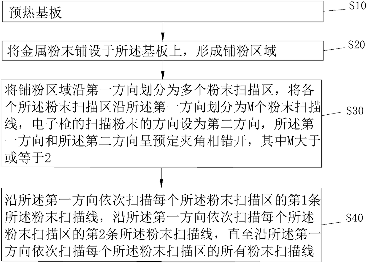
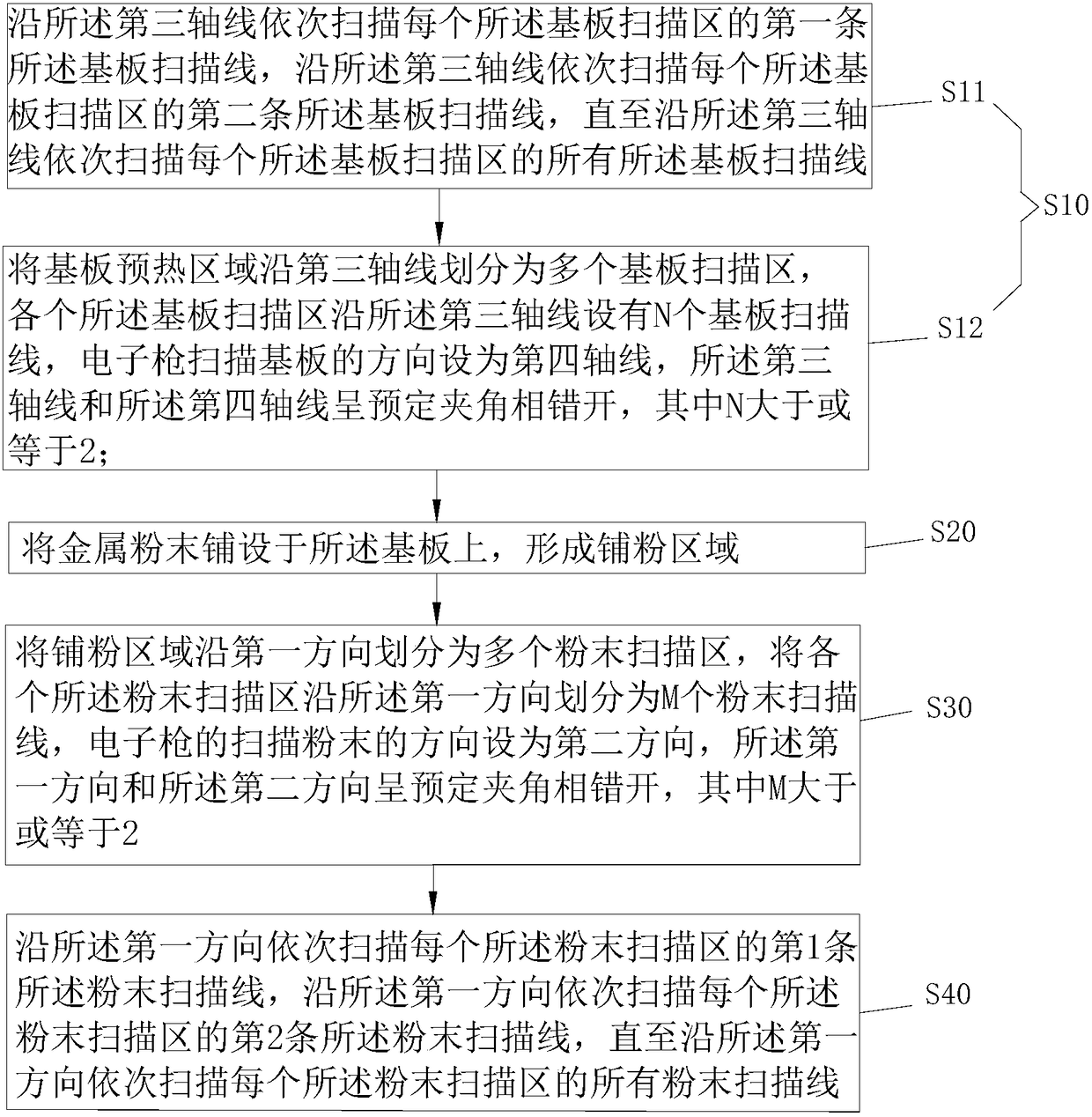
Scanning method for electronic beam selective melting
A technology of electronic area selection and scanning method, which is applied in the field of 3D printing, can solve problems such as pore defects and molding interruptions of molding parts, and achieve the effects of improving molding accuracy, uniform heating, and ensuring normal progress
- Summary
- Abstract
- Description
- Claims
- Application Information
AI Technical Summary
Problems solved by technology
Method used
Image

Examples
Embodiment Construction
[0027] In order to make the technical problems, technical solutions and beneficial effects to be solved by the present invention clearer, the following further describes the present invention in detail with reference to the accompanying drawings and embodiments. It should be understood that the specific embodiments described herein are only used to explain the present invention, but not to limit the present invention.
[0028] It should be noted that when an element is referred to as being "fixed to" or "disposed on" another element, it can be directly on the other element or indirectly on the other element. When an element is said to be "connected to" another element, it can be directly connected to the other element or indirectly connected to the other element.
[0029] It should be understood that the terms "length", "width", "upper", "lower", "front", "rear", "left", "right", "vertical", "horizontal", "top" , "Bottom", "Inner", "Outer" and other indications of the orientation ...
PUM
 Abstract
Description
Claims
Application Information
 - Generate Ideas
- Intellectual Property
- Life Sciences
- Materials
- Tech Scout
- Unparalleled Data Quality
- Higher Quality Content
- 60% Fewer Hallucinations
Browse by: Latest US Patents, China's latest patents, Technical Efficacy Thesaurus, Application Domain, Technology Topic, Popular Technical Reports.
© 2025 PatSnap. All rights reserved.Legal|Privacy policy|Modern Slavery Act Transparency Statement|Sitemap|About US| Contact US: help@patsnap.com