Display device and driving method thereof

A display device and display panel technology, applied to static indicators, instruments, etc., can solve problems such as incomplete grounding of data lines, failure to consider residual charges in pixel areas, abnormal charge display, etc.

Active Publication Date: 2018-06-15
NANJING CEC PANDA FPD TECH CO LTD
View PDF4 Cites 25 Cited by
  • Summary
  • Abstract
  • Description
  • Claims
  • Application Information

AI Technical Summary

Problems solved by technology

However, when the power supply voltage VDD or the analog positive voltage AVDD drops too fast, the data line will be incompletely grounded, and the residual charge in the data line cannot be fully released.
In addition, the above technical solutions do not take into account the residual charge inside the pixel region, such as the charge remaining at the interface of the pixel electrode, alignment film, etc.
[0006] And when the display device is turned on and off, the residual charge in the pixel area will cause instantaneous display abnormalities

Method used


Image

  • Display device and driving method thereof
  • Display device and driving method thereof
  • Display device and driving method thereof

Examples


Embodiment Construction

[0038] In order to more clearly illustrate the embodiments of the present invention or the technical solutions in the prior art, the specific implementation manners of the present invention will be described below with reference to the accompanying drawings. Obviously, the accompanying drawings in the following description are only some embodiments of the present invention, and those skilled in the art can obtain other accompanying drawings based on these drawings and obtain other implementations.

[0039] In order to make the drawing concise, each drawing only schematically shows the parts related to the present invention, and they do not represent the actual structure of the product. In addition, to make the drawings concise and easy to understand, in some drawings, only one of the components having the same structure or function is schematically shown, or only one of them is marked.

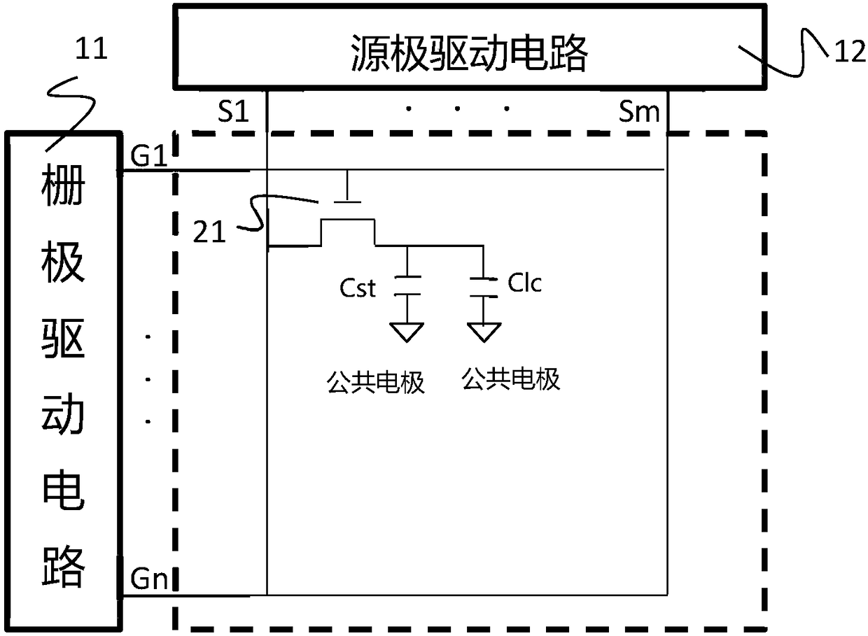
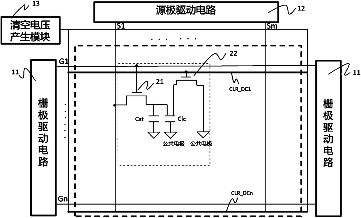
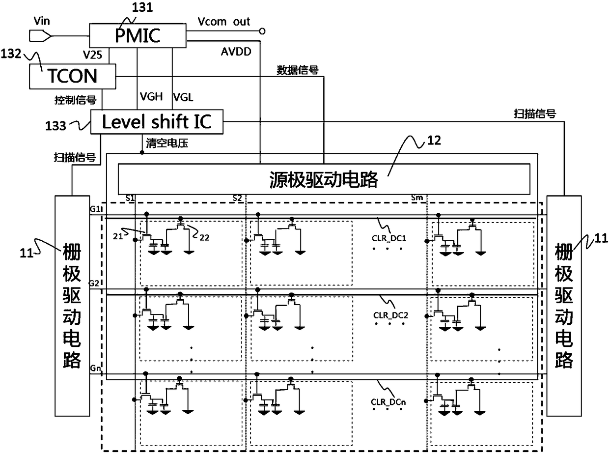
[0040] figure 2 It is a schematic diagram of the structure of the display device of the...


PUM


Abstract

The present invention discloses a display device and a driving method thereof. The display device comprises a display panel and a cleanup voltage generation module; the display panel comprises scanning lines and data lines which are criss-crossed, a common electrode, a pixel electrode, a plurality of pixel areas crosswise limited by the scanning lines and the data lines and a plurality of cleanupvoltage lines; the cleanup voltage generation module outputs cleanup voltages to the cleanup voltage lines and outputs a common voltage to the common electrode; each pixel area is internally providedwith a first thin film transistor and a second thin film transistor; the grid of each second thin film transistor is connected with the cleanup voltage lines, the source of each second thin film transistor is connected with the pixel electrode, and the drain of each second thin film transistor is connected with a common voltage line; and when the display device is shut down, the cleanup voltages are high level, the second thin film transistors are opened, the drains of the first thin film transistors and the pixel electrode connected with the drains of the first thin film transistors are in short connection with the common electrode, the display frame is a black state without a splash screen phenomenon; and the residual charges in the pixel area are completed released. The present invention further discloses a driving method of the display device.

Description

technical field [0001] The present invention relates to the field of display technology, in particular to a display device and a driving method thereof. Background technique [0002] Such as figure 1 As shown, the display device in the prior art is provided with criss-cross scan lines and data lines, and a pixel area defined by intersections of the scan lines and data lines, and a first thin film transistor 21 and a pixel electrode are provided in the pixel area. When the first thin film transistor 21 is turned off, the potential of the pixel area is mainly maintained by the liquid crystal capacitor Clc and the storage capacitor Cst. Due to charging and displaying images for a long time, charges will accumulate in the liquid crystal capacitors in the pixel area. [0003] When the display device is turned off, that is, when its power supply is turned off, all the first thin film transistors 21 are turned off, and some residual charges cannot be released immediately. Since ...

Claims


Application Information

Patent Timeline
Patent Type & Authority Applications(China)
IPC IPC(8): G09G3/20G09G3/36
CPCG09G3/20G09G3/36G09G3/3648
Inventor 叶纯邢程杨钰婷
Owner NANJING CEC PANDA FPD TECH CO LTD
Why Eureka
Try Eureka