Electronics Manufacturing Process

A manufacturing process and technology for electronic products, applied in semiconductor/solid-state device manufacturing, circuits, electrical components, etc., can solve problems such as inability to accurately absorb chips, uneven force on chips, and lower production efficiency, so as to reduce product defect rate, The effect of improving production efficiency and improving accuracy

Active Publication Date: 2020-05-19
重庆市长寿区普爱网络科技有限公司
View PDF4 Cites 0 Cited by
  • Summary
  • Abstract
  • Description
  • Claims
  • Application Information

AI Technical Summary

Problems solved by technology

[0004] At present, manufacturers often need to produce chips of different sizes and specifications, but at present when using ejector pins to jack up chips, the following defects often occur: 1. When using smaller-sized ejector pins to jack up larger-sized chips At this time, because the local stress area of ​​the chip is concentrated in the position where the chip is in contact with the ejector pin, the force on the chip is uneven, and the chip itself is very thin, so it is easy to cause problems such as chip breakage; 2. When using a larger size pusher When the ejector pin jacks up a small-sized chip, it is easy to lift up the chip next to it because the ejector pin is too large, resulting in the inability to accurately pick up the chip at the target position; and in order to avoid this problem, some factories use It is to manually replace the ejector pin to fit the size of the chip, but this method is too troublesome and reduces production efficiency

Method used


Image

  • Electronics Manufacturing Process
  • Electronics Manufacturing Process
  • Electronics Manufacturing Process

Examples


Embodiment 1

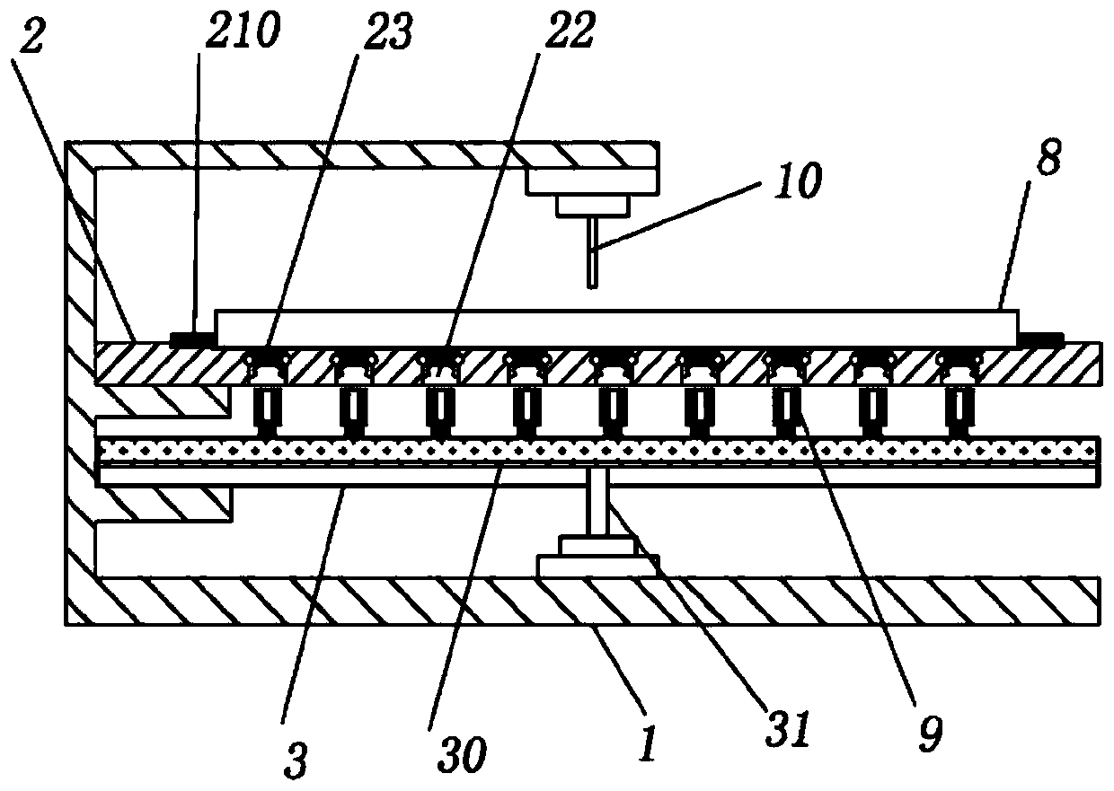
[0027] Basic as attached figure 1 Shown:

[0028] The electronic product manufacturing process adopts an ejector to eject chips, and the ejector includes a frame 1, a support table 2, an ejector mechanism 9, a hydraulic cylinder 3 and a push-pull part.

[0029] A dicing knife 10 for dicing the wafer 8 is telescopically connected above the frame 1 .

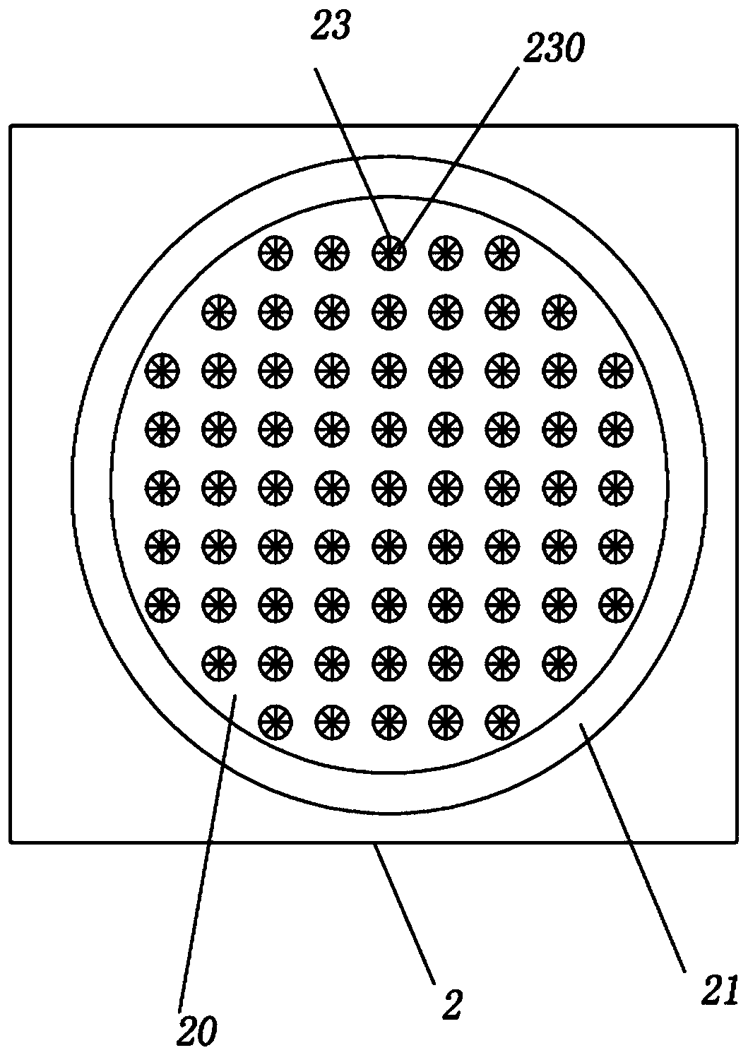
[0030] The support table 2 is used to support the wafer 8, such as figure 2 As shown, the shape of the support table 2 is a cube, and a circular groove 20 is provided in the center of the support table 2. The inner diameter of the groove 20 is consistent with the outer diameter of the wafer 8, so that after the wafer 8 is placed, Fixed wafer 8 effect. The circumferential direction of the groove 20 can also offer an iron ring placement groove 21, and the depth of the iron ring placement groove 21 is shallower than the depth of the groove 20, so that after putting the wafer 8 into the groove 20, the iron ring can also be placed ...

Embodiment 2

[0041] The difference between this embodiment and Embodiment 1 lies in that: the extrusion pressure of the hydraulic oil in step B is 15MPa; the suction pressure of the vacuum suction head in step C is 2KPa.


PUM


Abstract

The invention belongs to the technical field of production of electronic products, and specifically relates to an electronic product manufacturing process. An ejector is adopted to eject a chip, and the ejection step includes: A, opening a solenoid valve; B, starting a push-and-pull part; C, sucking a chip; and D, resetting. In Step A, an ejection rod of a corresponding size is selected accordingto the size of the chip, and the solenoid valve corresponding to the corresponding ejection rod is opened; in Step B, hydraulic oil in a hydraulic cylinder squeezes a push-and-pull piston in a pistoncylinder, and the ejection rod enters an ejection hole to eject the chip; in Step C, a vacuum sucker takes down the ejected chip; and in Step D, the hydraulic oil in the piston cylinder returns to thehydraulic cylinder through the push-and-pull part, the ejection rod is reset, and the solenoid valve is turned off. According to the scheme, when the chip is ejected, ejection rods of different sizescan be used aiming at chips of different sizes, a working procedure of manual replacement of the ejection rods can be avoided, and production efficiency is improved.

Description

technical field [0001] The invention belongs to the technical field of electronic product production, and in particular relates to an electronic product manufacturing process. Background technique [0002] Electronic products refer to electronic products used in daily consumer life. Chips, also known as microcircuits, microchips, and integrated circuits, refer to silicon chips containing integrated circuits. They are small in size and are the most important part of electronic products, undertaking the functions of computing and storage. The complete process of chip production includes several links such as chip design, wafer production, packaging production, and cost testing; the raw material for its production is wafers. Wafer refers to the silicon wafer used in the production of silicon semiconductor integrated circuits. Because of its circular shape, it is called a wafer; it can be processed into various circuit element structures on the silicon wafer, and become an IC w...

Claims


Application Information

Patent Timeline
Patent Type & Authority Patents(China)
IPC IPC(8): H01L21/67H01L21/683
CPCH01L21/67011H01L21/68714H01L21/68785
Inventor 李天翼
Owner 重庆市长寿区普爱网络科技有限公司
Why Eureka
Try Eureka