A polydimethylsiloxane three-dimensional microfluidic channel surface hydrophobic structure forming process

A technology of polydimethylsiloxane and molding process, which is applied in the direction of laboratory utensils, laboratory containers, chemical instruments and methods, etc., and can solve the problems of low processing efficiency, high cost of femtosecond lasers, and superhydrophobic surface Roughness and other problems, to achieve the effect of high production efficiency and low cost

Inactive Publication Date: 2019-12-13
GUANGDONG UNIV OF TECH +1
View PDF6 Cites 0 Cited by
  • Summary
  • Abstract
  • Description
  • Claims
  • Application Information

AI Technical Summary

Problems solved by technology

However, the cost of the femtosecond laser required by this method is extremely high, and the surface of the prepared superhydrophobic structure is very rough, and the processing efficiency is low.

Method used


Image

  • A polydimethylsiloxane three-dimensional microfluidic channel surface hydrophobic structure forming process

Examples


Embodiment

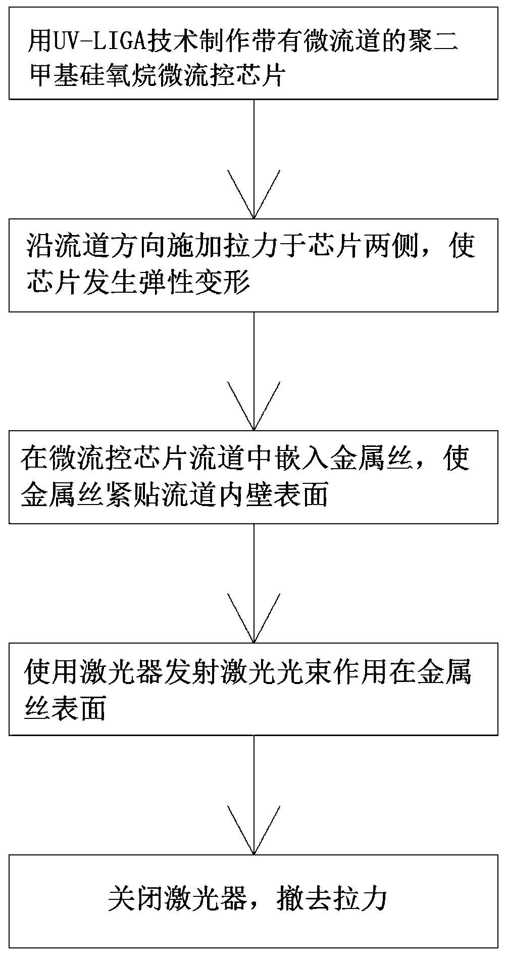
[0026] Embodiment: A polydimethylsiloxane three-dimensional microfluidic channel surface hydrophobic structure forming process.

[0027] A polydimethylsiloxane three-dimensional microfluidic channel surface hydrophobic structure forming process provided by the present invention comprises the following steps:

[0028] Step 1: Using UV-LIGA technology to fabricate a polydimethylsiloxane microfluidic chip with a microchannel, the width of the microchannel is 50 μm;

[0029] Step 2: Apply a pulling force of 0.5N on both sides of the chip along the direction of the flow channel to make the chip elastically deform;

[0030] Step 3: Embedding a metal wire with a diameter of 49 μm in the flow channel of the polydimethylsiloxane microfluidic chip in an elastically deformed state, so that the metal wire is close to the surface of the inner wall of the flow channel;

[0031] Step 4: Use a nanosecond fiber laser with a wavelength of 1064nm, a power of 10W, and a pulse frequency of 30kHz ...


PUM


Abstract

The invention provides a polydimethylsiloxane three-dimensional micro-channel surface hydrophobic structure forming process, which is mainly used in micro-droplet manipulation of micro-fluidic chips to solve the problems of fluid adhesion and two-phase fusion on the inner wall of micro-channels. The specific method is: (1) using UV-LIGA technology to make a polydimethylsiloxane microfluidic chip with a microchannel; (2) applying a pulling force on both sides of the chip along the direction of the channel; A metal wire with a diameter smaller than the width of the microchannel is embedded in the flow channel of the polydimethylsiloxane chip in an elastic deformation state; (4) the laser beam penetrates the polydimethylsiloxane material and acts on the surface of the metal wire; (5) Turn off the laser and remove the pulling force in a certain order; compared with the prior art, the nanosecond laser used in the present invention has low cost, high production efficiency, controllable hydrophobic area size and hydrophobic position, and the hydrophobic structure is a regular wavy wrinkle structure. The structure size can be tuned at the micro-nano scale.

Description

technical field [0001] The invention relates to the field of microfluidic chip production, in particular to a polydimethylsiloxane three-dimensional microfluidic channel surface hydrophobic structure forming process. Background technique [0002] The microfluidic chip is a miniaturized and integrated portable analysis device. The size of the flow channel is in the order of microns, and the analysis dose is measured in microliters. In some respects, the microfluidic channels in microfluidic chips need to undergo surface hydrophobic or hydrophilic modification to meet the actual application requirements. For example, in the application of micro-droplet manipulation, the superhydrophobic modification of the inner surface of the pipeline can greatly reduce the transport resistance of the flow channel, change the transport direction of the micro-droplet sample to be operated at will, and even cross one platform to another The platform performs three-dimensional operations. This...

Claims


Application Information

Patent Timeline
Patent Type & Authority Patents(China)
IPC IPC(8): B01L3/00
CPCB01L3/502707
Inventor 邓宇张会寅郭钟宁洪文生麦文豪王文兵朱紫红
Owner GUANGDONG UNIV OF TECH
Why Eureka
Try Eureka