Device and method for improving film thickness uniformity
A technology with uniform film thickness and wafer, applied in the direction of gaseous chemical plating, coating, electrical components, etc., can solve the problems of incomplete radio frequency shielding, radio frequency overlap, etc., to achieve the elimination of film thickness mutation, uniform film distribution, Effect of reducing film thickness difference
- Summary
- Abstract
- Description
- Claims
- Application Information
AI Technical Summary
Problems solved by technology
Method used
Image

Examples
Embodiment Construction
[0038] The specific embodiment of the present invention will be further described in detail below in conjunction with the accompanying drawings.
[0039] It should be noted that, in the following specific embodiments, when describing the embodiments of the present invention in detail, in order to clearly show the structure of the present invention for the convenience of description, the structures in the drawings are not drawn according to the general scale, and are drawn Partial magnification, deformation and simplification are included, therefore, it should be avoided to be interpreted as a limitation of the present invention.
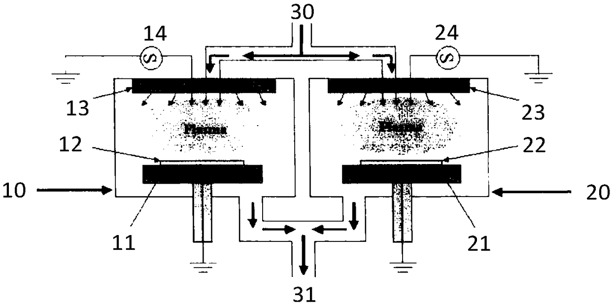
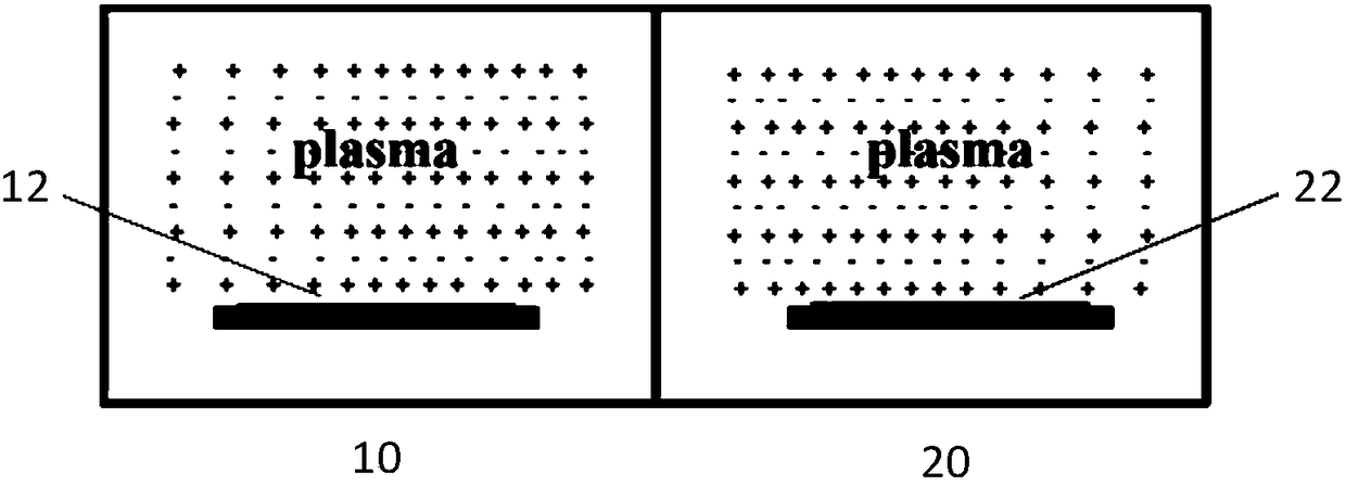
[0040] In the following specific embodiments of the present invention, please refer to Figure 4 , Figure 4 It is an exploded schematic view of a device for improving film thickness uniformity in a preferred embodiment of the present invention. Such as Figure 4As shown, a kind of device that improves film thickness uniformity of the present inve...
PUM
 Abstract
Description
Claims
Application Information
 - R&D Engineer
- R&D Manager
- IP Professional
- Industry Leading Data Capabilities
- Powerful AI technology
- Patent DNA Extraction
Browse by: Latest US Patents, China's latest patents, Technical Efficacy Thesaurus, Application Domain, Technology Topic.
© 2024 PatSnap. All rights reserved.Legal|Privacy policy|Modern Slavery Act Transparency Statement|Sitemap