OLED packaging method and packaging structure
A packaging structure and packaging method technology, which is applied in the manufacture of electrical components, electrical solid devices, semiconductor/solid devices, etc., can solve the problems of large thermal deformation differences, film layer peeling, and bubbling, so as to reduce film layer peeling or Bubble probability, elimination of thermal expansion and deformation differences, and effects of improving package reliability
- Summary
- Abstract
- Description
- Claims
- Application Information
AI Technical Summary
Problems solved by technology
Method used
Image

Examples
Embodiment Construction
[0033] The following descriptions of various embodiments refer to the accompanying drawings to illustrate specific embodiments in which the present invention can be implemented.
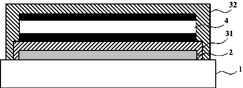
[0034] Please refer to image 3 As shown, Embodiment 1 of the present invention provides an OLED packaging structure, including:
[0035] Making a substrate 1 with an OLED device 2;
[0036] A first inorganic barrier layer 31 formed on the substrate 1 and covering the OLED device 2;
[0037] an organic buffer layer 4 formed on the first inorganic barrier layer 31, the organic buffer layer 4 doped with particles having a negative thermal expansion coefficient; and
[0038] The second inorganic barrier layer 32 is formed on the substrate 1 and covers the first inorganic barrier layer 31 and the organic buffer layer 4 .
[0039] It can be seen from the foregoing that the thermal expansion coefficients of the organic buffer layer (organic buffer layer) and the inorganic barrier layer (inorganic barrie...
PUM
| Property | Measurement | Unit |
|---|---|---|
| Thickness | aaaaa | aaaaa |
| Thickness | aaaaa | aaaaa |
Abstract
Description
Claims
Application Information
 - R&D
- Intellectual Property
- Life Sciences
- Materials
- Tech Scout
- Unparalleled Data Quality
- Higher Quality Content
- 60% Fewer Hallucinations
Browse by: Latest US Patents, China's latest patents, Technical Efficacy Thesaurus, Application Domain, Technology Topic, Popular Technical Reports.
© 2025 PatSnap. All rights reserved.Legal|Privacy policy|Modern Slavery Act Transparency Statement|Sitemap|About US| Contact US: help@patsnap.com