
Wiring structure of printed circuit board

A printed circuit board and wiring structure technology, which is applied in the direction of printed circuit, printed circuit, printed circuit components, etc., can solve the problems of low cost of printed circuit board, damage to the environment of ground wire and ground wire, and degradation of device performance. To achieve the effect of ensuring the impedance environment

Inactive Publication Date: 2018-08-14
AMOLOGIC (SHANGHAI) CO LTD
View PDF3 Cites 7 Cited by
  • Summary
  • Abstract
  • Description
  • Claims
  • Application Information

AI Technical Summary

Problems solved by technology

[0004] The cost of double-layer printed circuit boards is low, but it is easy to generate high impedance, especially when different connections need to cross, which will destroy the ground environment formed by the ground wire, and may also destroy the impedance environment of the signal line at the same time. leading to a decrease in the performance of the formed device

Method used


Image

  • Wiring structure of printed circuit board

Examples


Embodiment Construction

[0020] The present invention will be further described below in conjunction with the accompanying drawings and embodiments.

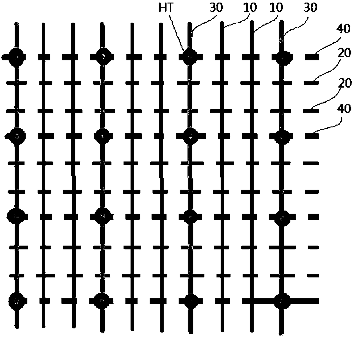
[0021] In a preferred embodiment, as figure 1 As shown, a wiring structure of a printed circuit board is proposed, which is applied to a printed circuit board, wherein the printed circuit board is a double-layer structure with a top layer and a bottom layer: the wiring structure includes:

[0022] A plurality of first signal lines 10 and a plurality of first ground lines 30, each of the first signal lines 10 and the first ground lines 30 are distributed in parallel on the top layer and extend along a first direction;

[0023] A plurality of second signal lines 20 and a plurality of second ground lines 40, each of the second signal lines 20 and the second ground lines 40 are distributed in parallel on the bottom layer and extend along a second direction different from the first direction;

[0024] Wherein, the first signal line 10 and the first ground w...


PUM


Abstract

The invention relates to the technical field of an integrated circuit, in particular to a wiring structure of a printed circuit board. The wiring structure is applied to a dual-layer printed circuit board and comprises a plurality of first signal lines, a plurality of first ground lines, a plurality of second signal lines and a plurality of second ground lines, wherein each first signal line and each first ground line are arranged at a top layer in parallel and extend along a first direction, each second signal line and each second ground line are arranged at a bottom layer in parallel and extend along a second direction different from the first direction, the first signal lines and the first ground lines are arranged at the top layer at intervals according to a first preset mode, the second signal lines and the second ground lines are arranged at the bottom layer at intervals according to the second preset mode, and the first ground lines and the second ground lines are connected through via holes in the printed circuit board. By the wiring structure, the situation that a ground line environment is damaged caused by connection line crossing can be prevented, meanwhile, the impedance environment of the signal lines is ensured, and the performance of a circuit on the printed circuit board is ensured under the condition that the cost is not increased.

Description

technical field [0001] The invention relates to the technical field of integrated circuits, in particular to a wiring structure of a printed circuit board. Background technique [0002] PCB (Printed Circuit Board, PCB for short) is an important electronic component, a support for electronic components, and a carrier for electrical connections of electronic components. [0003] Printed circuit boards have developed from single-layer to double-sided, multi-layer and flexible, and still maintain their own development trends. Due to the continuous development in the direction of high precision, high density and high reliability, continuous reduction in size, cost reduction and performance improvement, printed boards still maintain strong vitality in the development of future electronic equipment. [0004] The cost of double-layer printed circuit boards is low, but it is easy to generate high impedance, especially when different connections need to cross, which will destroy the ...

Claims


Application Information

Patent Timeline
Patent Type & Authority Applications(China)
IPC IPC(8): H05K1/02
CPCH05K1/025H05K2201/0776H05K2201/09227
Inventor 张坤
Owner AMOLOGIC (SHANGHAI) CO LTD
Learn More