Manufacturing method of oriented film and display panel

A manufacturing method and technology for display panels, which are applied in optics, instruments, nonlinear optics, etc., can solve the problem that it is difficult to meet the narrow frame of TFT-LCD panels, and achieve the effect of good film thickness uniformity.

Inactive Publication Date: 2018-08-24
BOE TECH GRP CO LTD +1
View PDF6 Cites 2 Cited by
  • Summary
  • Abstract
  • Description
  • Claims
  • Application Information

AI Technical Summary

Problems solved by technology

[0004] However, considering the influence of polyimide liquid diffusion, its patterning accuracy can usually only reach between 500-1500 μm, which is difficult to meet the narrow frame requirements of existing TFT-LCD panels. The difference in thickness between the edge and the central area of ​​natural diffusion is obvious, and there are many problems in the quality of the edge display

Method used


Image

  • Manufacturing method of oriented film and display panel
  • Manufacturing method of oriented film and display panel
  • Manufacturing method of oriented film and display panel

Examples


Embodiment Construction

[0032] The technical solutions of the present invention will be further described below according to specific embodiments. The protection scope of the present invention is not limited to the following examples, which are listed for illustrative purposes only and do not limit the present invention in any way.

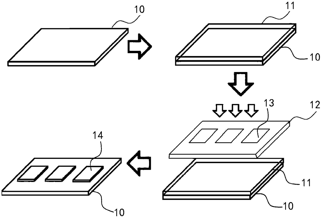
[0033] It should be understood that the drawings disclosed herein are not necessarily drawn according to the scale of actual devices and components. The shapes and thicknesses of the embodiments may be exaggerated in the drawings in order to clearly show the features of the embodiments of the present invention. In addition, the structures and devices in the drawings are shown schematically in order to clearly show the features of the embodiments of the present invention.

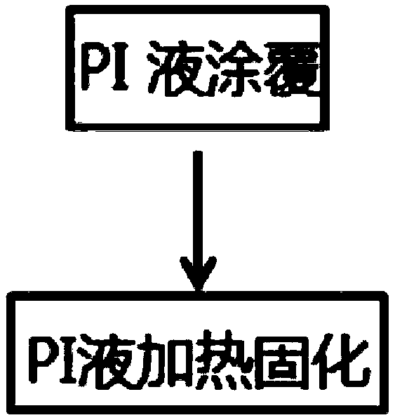
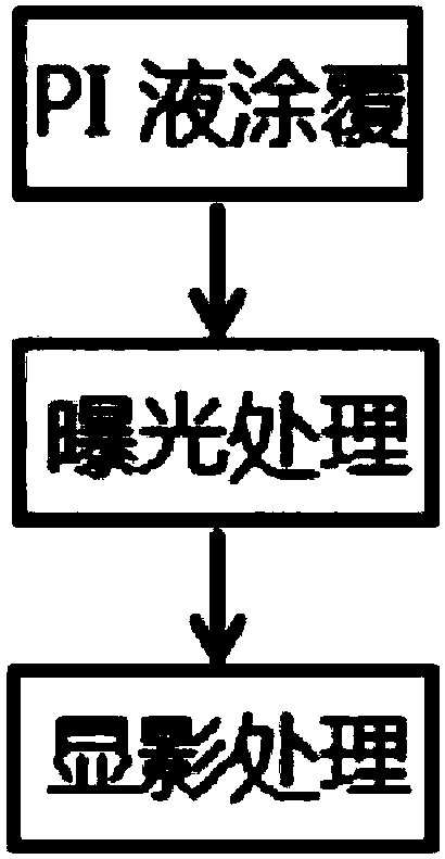
[0034] figure 2 It is a flowchart of a method for manufacturing an alignment film according to an embodiment of the present invention, such as figure 2 As shown, the manufacturing method of the al...


PUM


Abstract

The invention provides a manufacturing method of an oriented film and a display panel. The method includes the steps of forming a photosensitive polyimide layer on a substrate, conducting exposure treatment on the polyimide layer through a mask plate, and conducting developing treatment on the exposed polyimide layer to obtain the oriented film. Compared with existing process conditions, the patterning precision of the manufactured oriented film can reach the micron order so that the requirements of an existing TFT-LCD panel narrow frame can be met; meanwhile, since polyimide is subjected to patterning treatment after being coated overall, the oriented film is higher in film thickness uniformity and can not influence the quality of images displayed on the edge.

Description

technical field [0001] The invention relates to the display field, in particular to a method for manufacturing an alignment film and a display panel. Background technique [0002] In the manufacturing process of TFT-LCD (thin film transistor-liquid crystal display), it is necessary to set an alignment film on the array substrate and the color filter substrate of the thin film crystal liquid crystal display, and the alignment film is processed to form grooves along a certain direction to make the liquid crystal aligned along the groove direction. Alignment film materials have good properties such as chemical corrosion resistance and electrical insulation. However, some areas of the TFT panel itself cannot be coated with PI, which requires patterned coating on the substrate. [0003] Such as figure 1 As shown, at present, the alignment film is mainly formed by patterned coating of polyimide liquid, and then it is heated and cured to form an alignment film with a predetermine...

Claims


Application Information

Patent Timeline
Patent Type & Authority Applications(China)
IPC IPC(8): G02F1/1337
CPCG02F1/133723G02F1/133788
Inventor 张俊伟王洋李官正何成勇李金祥
Owner BOE TECH GRP CO LTD
Why Eureka
Try Eureka