Liquid crystal display device and viewing angle switching method thereof
A technology of liquid crystal display device and viewing angle, applied in static indicators, instruments, nonlinear optics, etc.
- Summary
- Abstract
- Description
- Claims
- Application Information
AI Technical Summary
Problems solved by technology
Method used
Image


Examples
no. 1 example
[0031] figure 1 It is a schematic plan view of the liquid crystal display device in the first embodiment of the present invention, figure 2 for figure 1 The schematic diagram of the local structure in image 3 for figure 1 Schematic diagram of the structure of the middle viewing angle control electrode, Figure 4 for figure 1 Schematic diagram of the breakdown structure in . Please refer to Figure 1 to Figure 4 , the liquid crystal display device includes a first substrate 21 , a second substrate 22 opposite to the first substrate 21 , and a liquid crystal layer 23 between the first substrate 21 and the second substrate 22 .
[0032] The liquid crystal display device provided in this embodiment is suitable for liquid crystal display devices in modes such as in-plane switching (IPS) and fringe field switching (FFS), and the common electrode and the pixel electrode are all formed on the same substrate (ie, a thin film transistor array substrate). When an electric field ...
no. 2 example
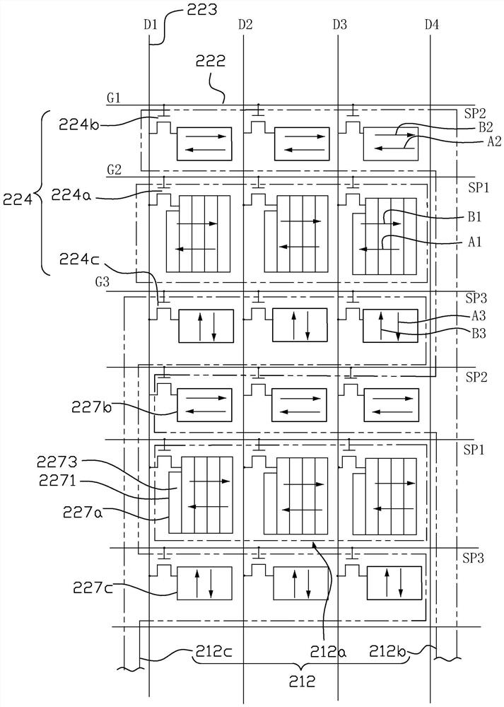
[0056] Figure 6 It is a schematic plan view of the liquid crystal display device in the second embodiment of the present invention, Figure 7 for Figure 6 The schematic diagram of the decomposition structure in, Figure 8a to Figure 8d for Figure 6 Schematic diagram of the alignment of neutral liquid crystal molecules when different voltages are applied to the viewing angle control electrode. The difference between this embodiment and the first embodiment is that in this embodiment, the liquid crystal layer 23 adopts positive liquid crystal molecules.
[0057] Please combine Figure 6 and Figure 7 , the alignment direction of the position corresponding to each primary pixel SP1 on the first substrate 21 is A1, the alignment direction of the position corresponding to each primary pixel SP2 on the first substrate 21 is A2, and the alignment direction of each primary pixel SP2 on the first substrate 21 is The alignment direction of the position corresponding to each secon...
no. 3 example
[0068] Figure 9 It is a partial cross-sectional view of the liquid crystal display device in the third embodiment of the present invention. Please refer to image 3 , the difference between this embodiment and the second embodiment is that a common electrode 225 is provided on the second substrate 22 corresponding to each primary pixel SP1, and the second substrate 22 corresponds to each primary pixel SP2 and each primary pixel SP2. The area of the second sub-pixel SP3 is not provided with the common electrode 225 . For other structures and components included in this embodiment, please refer to the second embodiment.
[0069] When a display voltage is applied to the pixel electrode 227, and no voltage difference or a small voltage difference is applied between the first electrode portion 212a and the common electrode 225, and between the second electrode portion 212b, the third electrode portion 212c and the pixel When a certain voltage difference is applied between the...
PUM
 Abstract
Description
Claims
Application Information