Chamber and plasma processing device

A chamber and flow chamber technology, applied in the direction of discharge tubes, electrical components, circuits, etc., can solve problems such as discharge in the flow chamber, and achieve the effect of expanding the process window and the scope of application

Active Publication Date: 2018-09-14
BEIJING NAURA MICROELECTRONICS EQUIP CO LTD
View PDF6 Cites 6 Cited by
  • Summary
  • Abstract
  • Description
  • Claims
  • Application Information

AI Technical Summary

Problems solved by technology

[0005] The present invention aims at the above-mentioned deficiencies existing in the prior art, and provides a chamber and a plasma processing device to solve the problem of discharge in the uniform flow chamber

Method used


Image

  • Chamber and plasma processing device
  • Chamber and plasma processing device
  • Chamber and plasma processing device

Examples


Embodiment Construction

[0038] The technical solutions in the present invention will be clearly and completely described below in conjunction with the accompanying drawings in the present invention. Apparently, the described embodiments are part of the embodiments of the present invention, not all of them. Based on the embodiments of the present invention, all other embodiments obtained by persons of ordinary skill in the art without making creative efforts belong to the protection scope of the present invention.

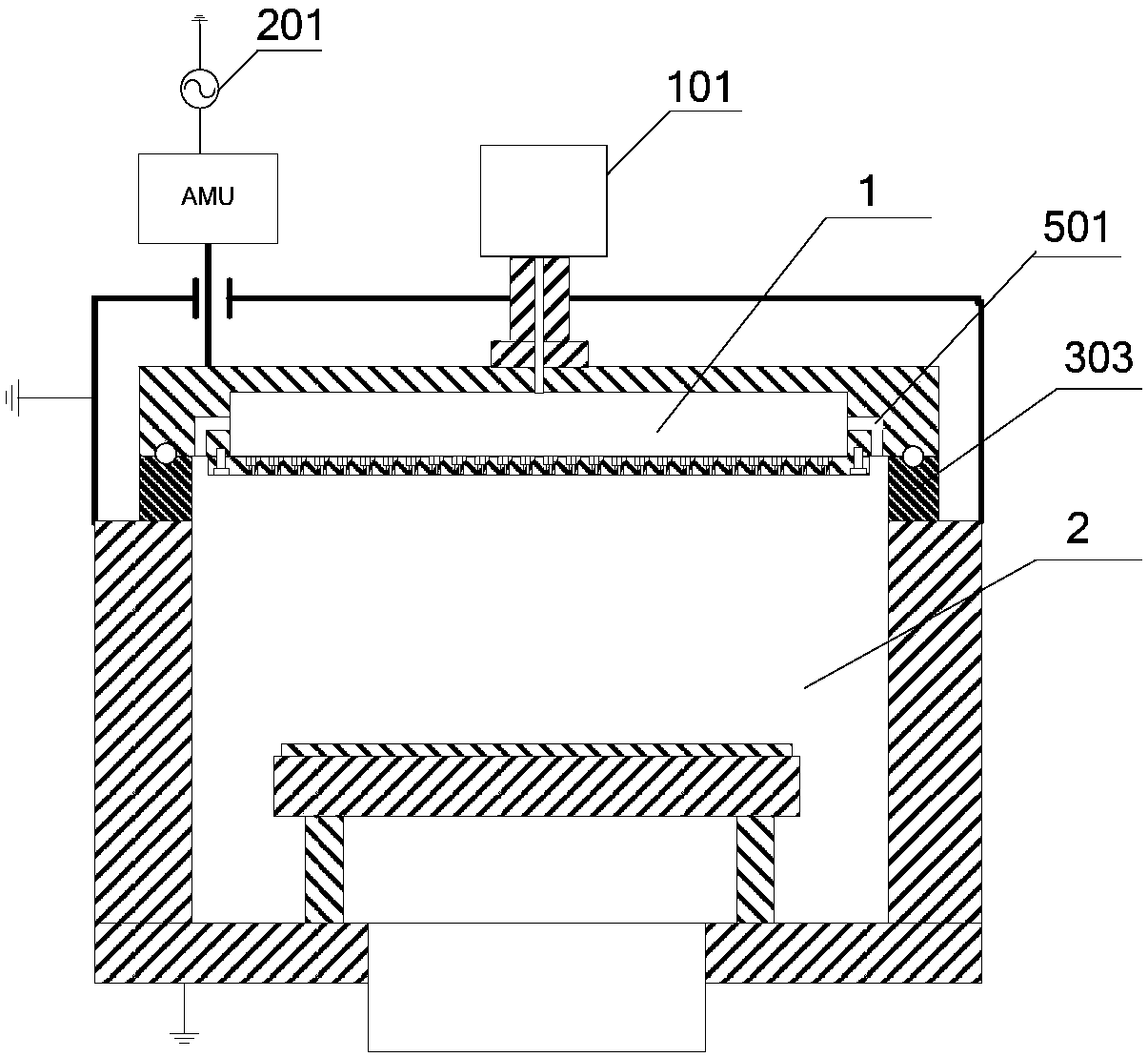
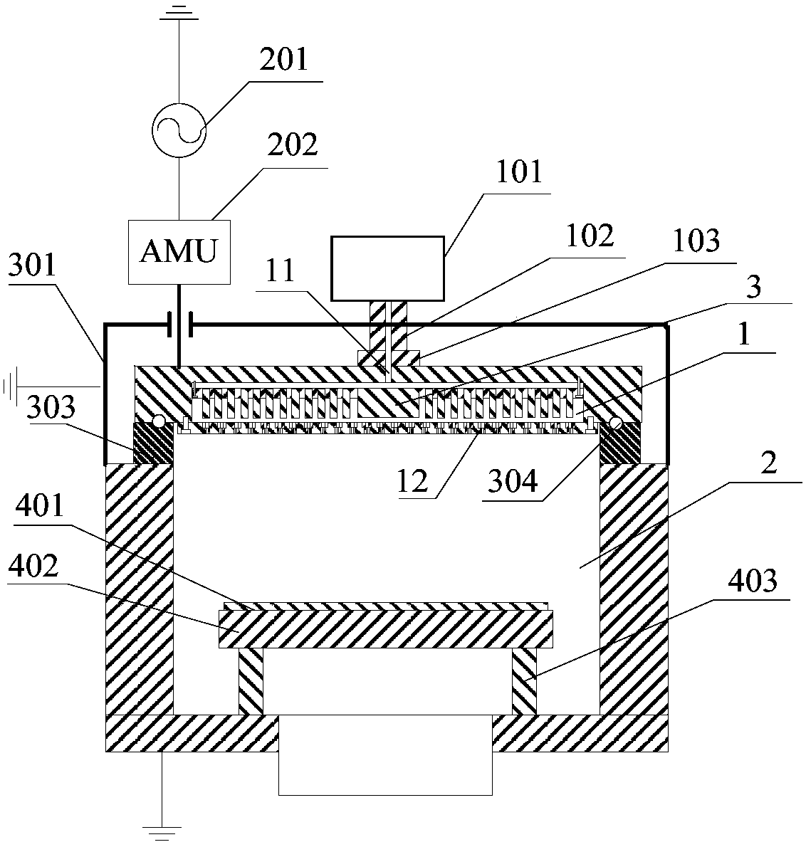
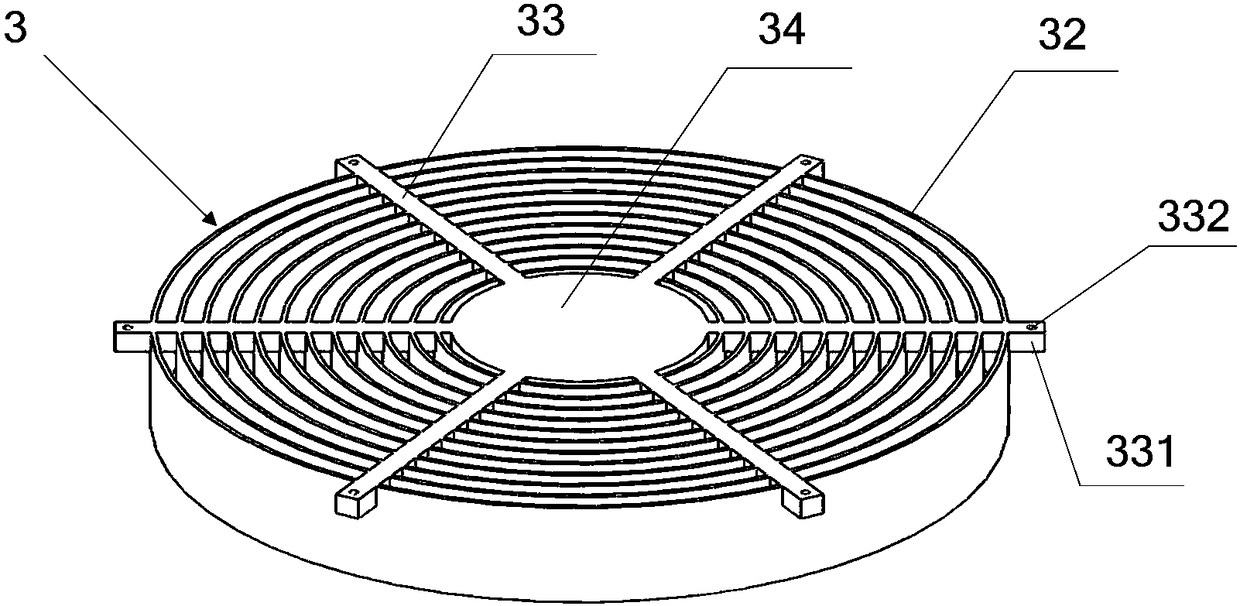
[0039] In the embodiment of the present invention, by setting a grid structure in the uniform flow chamber, by controlling the distance between the grid structure and the inner wall of the uniform flow chamber, and the distance between the grid plates of the grid structure, avoiding A discharge phenomenon occurs.

[0040] Combine the following Figure 2 to Figure 4b , to describe the technical solution of the present invention in detail.

[0041] Such as figure 2 As shown, the present ...


PUM


Abstract

The invention provides a chamber and a plasma processing device. A gate structure composed of multiple grid plates is disposed in a uniform flow chamber, the product of the first distance d1 between the gate structure and the top wall of the uniform flow chamber and the pressure p in the flow chamber, the product of the second distance d2 between the gate structure and the bottom wall of the uniform flow chamber and the pressure p in the uniform flow chamber and the product of the third distance d3 between adjacent grid plates and the pressure p in the uniform flow chamber are all less than 1.33pa*m or are all greater than 13.3pa*m, so discharge in the uniform flow chamber can be avoided. Even if the radio frequency power is relatively high or the air pressure is relatively high, the gatestructure can still work normally, so the process window and the applicable range can be expanded, especially for high pressure and high power process conditions.

Description

technical field [0001] The invention relates to the technical field of semiconductor equipment manufacturing, in particular to a chamber and a plasma processing device. Background technique [0002] Plasma Enhanced Chemical Vapor Deposition (Plasma Enhanced Chemical Vapor Deposition, PECVD) is one of the important means of preparing thin films using plasma technology. It is a method of ionizing the reaction gas with the help of plasma, so that the active substances such as free radicals and ions generated by the reaction gas produce chemical reactions in the gas phase or on the surface of the substrate, and finally deposit a thin film on the substrate. In PECVD devices, flat plate capacitive coupling discharge is widely used in semiconductor, photovoltaic and other industrial fields due to its advantages of large-area substrate support and good film growth uniformity. [0003] figure 1 It is an existing PECVD chamber structure. The PECVD chamber includes a uniform flow ch...

Claims


Application Information

Patent Timeline
Patent Type & Authority Applications(China)
IPC IPC(8): H01J37/32
CPCH01J37/32431H01J37/32458
Inventor 李兴存
Owner BEIJING NAURA MICROELECTRONICS EQUIP CO LTD
Why Eureka
Try Eureka