
A photo-controlled thyristor with a deep n+ hole current blocking layer

A light-controlled thyristor and hole current technology, which is applied in the direction of circuits, electrical components, semiconductor devices, etc., can solve the problems of large peak current, large total power of light-controlled thyristor devices, device damage and failure, etc.

Active Publication Date: 2019-09-27
UNIV OF ELECTRONICS SCI & TECH OF CHINA
View PDF7 Cites 0 Cited by
  • Summary
  • Abstract
  • Description
  • Claims
  • Application Information

AI Technical Summary

Problems solved by technology

More importantly, due to the large total power, large peak current, and high current rise rate (di / dt) of photo-controlled thyristor devices used in pulse power applications, if the device design is not good, it may cause the device to be damaged due to excessive local current density. damage to failure
The front of the light-controlled thyristor is composed of a grating, an amplifying gate, and a main cathode area. During the triggering and opening process of the device, the current flows through the P base area under the amplifying gate to make the PN junction at the amplifying gate reach the voltage threshold and turn on, further realizing current amplification, and finally The current transported laterally to the cathode area is particularly large. If the current in the cathode area cannot be evenly distributed, it may cause partial failure of the cathode area of ​​the device due to excessive current.

Method used


Image

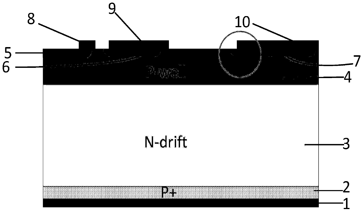
  • A photo-controlled thyristor with a deep n+ hole current blocking layer
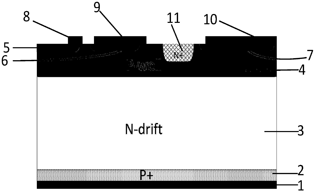
  • A photo-controlled thyristor with a deep n+ hole current blocking layer
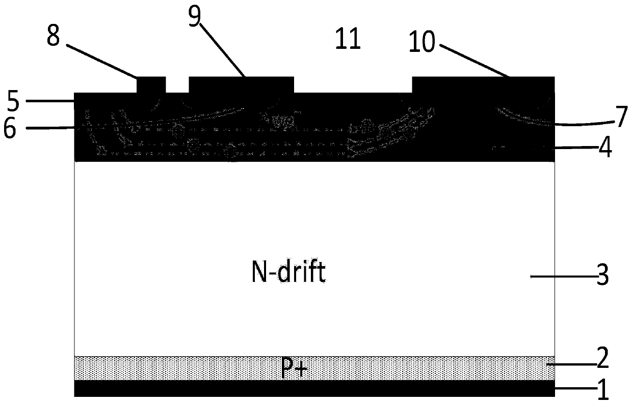
  • A photo-controlled thyristor with a deep n+ hole current blocking layer

Examples


Embodiment

[0024] Taking the conventional photothyristor with a withstand voltage of 6000V and the deep N+ hole current blocking layer provided by the present invention as examples, the performance advantages of the present invention in the pulse power application field compared with conventional LTTs are intuitively demonstrated. In order to verify the advantages of the deep N+ hole current blocking layer photo-controlled thyristor provided by the present invention in the field of pulse power application, two devices are simulated with the device simulation software Sentaurus. The original cell width of the two devices is taken as 400μm, and the chip area of ​​the device is taken as 0.5cm in the transient simulation 2 .

[0025] The topological circuit of the device working during transient simulation is as follows: Figure 5 As shown, the device works under the LRC oscillation circuit, where Vs is 6000V, R1 is 100Ω, R2 is 0.01Ω, inductance L is 10nH, capacitor C is 1μF, and anti-paral...


PUM


Abstract

The invention relates to the technology of semiconductors, in particular to an optical control thyristor with a deep N+ hole current blocking layer. The invention provides a design example of the optical control thyristor with the deep N+ hole current blocking layer. By changing a hole current circulation path, hole current is allowed to relieving a current centralization region in the device around a current centralization region on the left side of a cathode so as to allow the current distribution is quite even, thereby improving current resisting rising rate of the device. In addition, dueto the own characteristics, adjustment is performed according to the specific designing scheme of cellular. The beneficial effects are that an LTT device design of the deep N+ blocking layer is provided, so an invalidation problem of a conventional LTT device caused by centralization of current of the left side region of the main cathode is solved. Meanwhile, manufacturing technology which is thesame as that of the conventional device is provided. The thyristor is especially suitable for an optical control thyristor with big pulse power application and with high peak value current ability andhigh current increasing ability.

Description

technical field [0001] The invention relates to semiconductor technology, in particular to a light-controlled thyristor with a deep N+ hole current blocking layer. Background technique [0002] Power semiconductor devices, as switching devices, can be applied in both the power electronics field and the pulse power field. In the field of power electronics, the traditional Light Triggered Thyristor (LTT for short) is widely used as a pulse discharge switching device due to its superior performance. In the field of power electronics applications, the development trend of photo-controlled thyristor device technology is to use cathode short-circuit structure to improve withstand voltage, and at the same time control the size and number of cathode short-circuit structures. At the same time, researchers also provide some new device structures and process technologies to achieve high current capacity and meet the requirements of pulse power application capabilities. [0003] In pu...

Claims


Application Information

Patent Timeline
Patent Type & Authority Patents(China)
IPC IPC(8): H01L31/111H01L31/0352
Inventor 陈万军邓操夏云高吴昊左慧玲刘超
Owner UNIV OF ELECTRONICS SCI & TECH OF CHINA
Learn More