Encapsulation STRUCTURE AND THE MANUFACTURE THEREOF

A technology of packaging structure and manufacturing method, applied in semiconductor/solid-state device manufacturing, electrical components, electrical solid-state devices, etc., can solve the problems of high manufacturing cost, complicated manufacturing process, reliability problems, etc., and achieve the goal of reducing manufacturing cost and simplifying the manufacturing process Effect

Inactive Publication Date: 2018-10-09
SILICONWARE PRECISION IND CO LTD
View PDF8 Cites 0 Cited by
  • Summary
  • Abstract
  • Description
  • Claims
  • Application Information

AI Technical Summary

Problems solved by technology

[0005] However, in the manufacturing method of the existing packaging structure 1, the flip-chip process is adopted, and the manufacturing process is complicated, such as forming the primer 14, resulting in high manufacturing cost
[0006] In addition, since the sensing surface 11a is exposed outward when the encapsulant 13 is formed, the adhesive material 13' of the encapsulant 13 will overflow (Mold Flash) onto the sensing surface 11a and contaminate the sensing surface. Surface 11a, so terminal electronic products (such as computers, mobile phones, etc.) using this packaging structure 1 will have reliability problems

Method used


Image

  • Encapsulation STRUCTURE AND THE MANUFACTURE THEREOF
  • Encapsulation STRUCTURE AND THE MANUFACTURE THEREOF
  • Encapsulation STRUCTURE AND THE MANUFACTURE THEREOF

Examples


Embodiment Construction

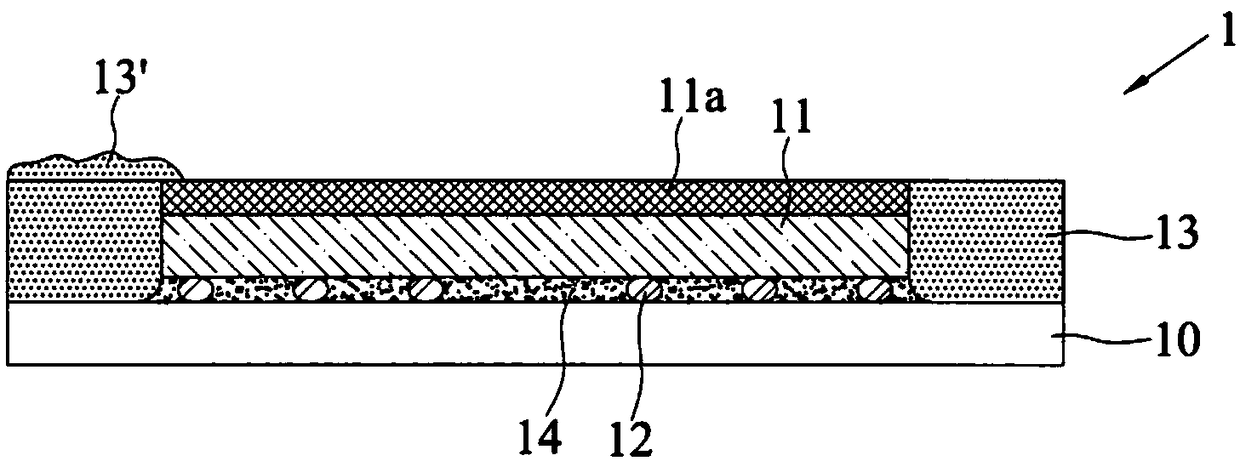
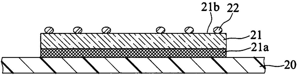
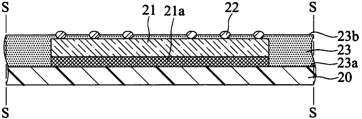
[0043] Embodiments of the present invention are described below through specific examples, and those skilled in the art can easily understand other advantages and effects of the present invention from the content disclosed in this specification. The present invention can also be implemented or applied through other different specific examples, and various modifications and changes can be made to the details in this specification based on different viewpoints and applications without departing from the spirit of the present invention.

[0044] It should be noted that the structures, proportions, sizes, etc. shown in the drawings attached to this specification are only used to match the content disclosed in the specification for the understanding and reading of those skilled in the art, and are not used to limit the implementation of this creation. There are limited conditions, so it has no technical substantive significance. Any modification of structure, change of proportional ...


PUM


Abstract

An encapsulation structure and its manufacturing method are used for attaching a sensing electronic element to a bearing piece with its sensing surface, forming an encapsulation layer for encapsulating the electronic element on the bearing piece, and exposing the sensing surface of the electronic element to the encapsulation layer after removing the bearing piece. Therefore, the encapsulation process is replaced, and the process cost is reduced.

Description

technical field [0001] The present invention relates to a packaging structure, in particular to a sensor packaging structure. Background technique [0002] As consumers pay more attention to privacy, many high-end electronic products have been equipped with user identification systems to increase the security of data in electronic products. Therefore, the research and development and design of identification systems have become electronic One of the main development directions of the industry. [0003] In the biometric identification system, it can be broadly divided into biometric identification systems that identify biological characteristics (such as fingerprints, pupils, faces, and voiceprints) and behavioral characteristics (such as signatures and voices) according to different identification targets. Among them, the identification system for identifying physiological characteristics has the advantages of singleness, high degree of anti-counterfeiting and convenience, ...

Claims


Application Information

Patent Timeline
IPC IPC(8): H01L23/31H01L21/56
CPCH01L21/56H01L23/3185H01L2224/73253
Inventor 唐绍祖王隆源陈美琪蔡瀛洲
Owner SILICONWARE PRECISION IND CO LTD
Why Eureka
Try Eureka