A Pad Structure

A pad and contact structure technology, applied in semiconductor/solid-state device parts, semiconductor devices, electrical components, etc., can solve problems such as failure, device performance and yield reduction, damage to pad devices, etc.

Active Publication Date: 2020-07-28
SEMICON MFG INT (BEIJING) CORP +1
View PDF9 Cites 0 Cited by
  • Summary
  • Abstract
  • Description
  • Claims
  • Application Information

AI Technical Summary

Problems solved by technology

However, as the size of the through hole becomes larger, PID will damage the device under the pad, which will reduce the performance and yield of the device, or even fail

Method used


Image

  • A Pad Structure
  • A Pad Structure

Examples


Embodiment 1

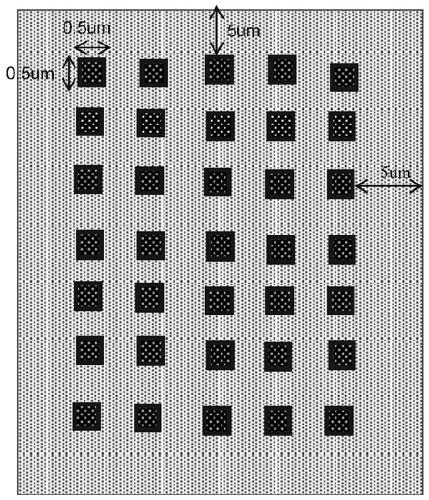
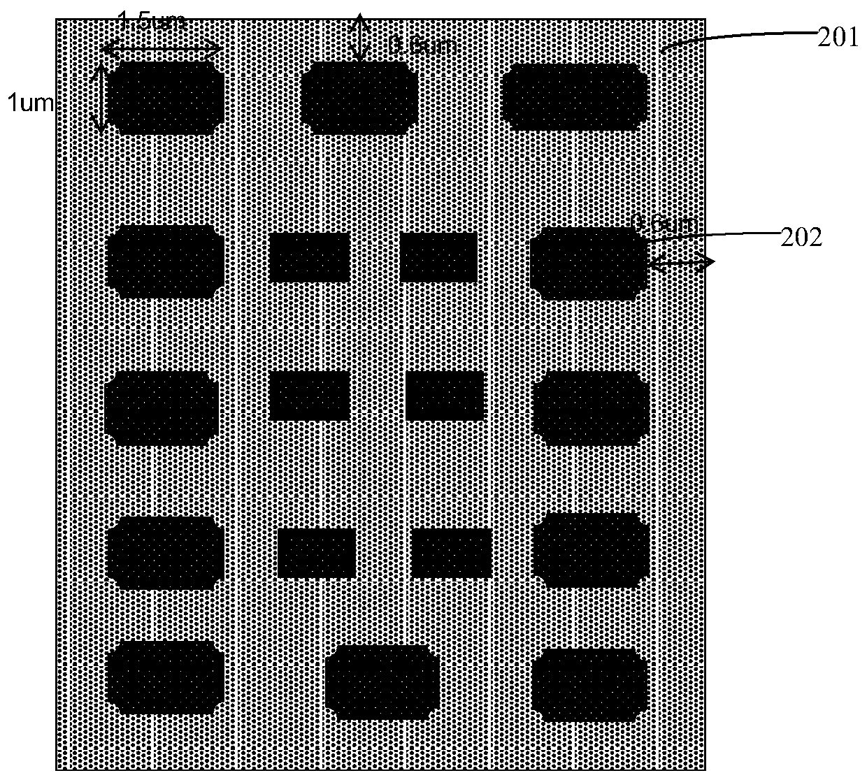
[0042] The preparation method of the semiconductor device of the present invention is described in detail below with reference to the accompanying drawings, figure 1 A top view of a pad structure in the prior art is shown; figure 2 A top view of a pad structure in an embodiment of the present invention is shown.

[0043] In order to solve the current problems, it is necessary to ensure that the top view area of ​​the through hole, that is, the contact structure will not decrease, while the side wall area of ​​the contact structure will decrease. Therefore, the present invention provides a solution based on the above research and analysis. A pad structure such as figure 2 As shown, the pad structure includes a contact structure 202 and a pad layer 201 disposed on the contact structure for electrical connection, and the contact structure includes several contact units arranged at intervals;

[0044] At least one of the contact units is integrally formed with another contact ...


PUM


Abstract

The invention provides a bonding pad structure. The bonding pad structure comprises a contact structure and a bonding pad layer which is arranged on the contact structure so as to realize electrical connection, wherein the contact structure comprises a plurality of contact units arranged at intervals; at least one of the contact units is integrally formed with another contact unit so as to form acontact unit with increased projection area on the bonding pad layer; or, at least one of the contact units is longitudinally divided into N parts, the N parts are integrally formed with the N contactunits so as to form the N contact units with increased projection area on the bonding pad layer, and N is greater than or equal to 2. According to the bonding pad structure, due to the fact that thetotal area of the projection, on the bonding pad layer, of the contact structure does not change, so that the current density does not change under larger current, and the fusion of the contact structure cannot be caused; and moreover, the total area of the side wall of the contact structure can be reduced by reducing the quantity of the contact structures, and then the damage effect of plasma isreduced.

Description

technical field [0001] The present invention relates to the technical field of semiconductors, in particular to a bonding pad structure. Background technique [0002] For the VLSI manufacturing industry, with the continuous reduction in the size of MOSFET (Metal Oxide Semiconductor Field Effect Transistor) devices, the semiconductor manufacturing process has entered the era of deep submicron, and is developing towards ultra-deep submicron. At this time, The reliability of semiconductor devices directly affects the performance and service life of IC chips produced. [0003] In the manufacturing process of semiconductor devices, many process steps such as dry etching, ion implantation, and chemical vapor deposition use plasma. In theory, the plasma is electrically neutral to the outside, that is, positive and negative ions The numbers are equal. But in fact, the positive ions and negative ions entering the local area of ​​the wafer are not equal, which leads to the generatio...

Claims


Application Information

Patent Timeline
Patent Type & Authority Patents(China)
IPC IPC(8): H01L23/488
CPCH01L24/05H01L2224/05012H01L2224/0502
Inventor 牛刚
Owner SEMICON MFG INT (BEIJING) CORP
Why Eureka
Try Eureka