Display panel, manufacturing method thereof and display device

A display panel and substrate technology, applied in nonlinear optics, instruments, optics, etc., can solve the problems affecting the aperture ratio of the display panel, the color shift of the display panel, the difference in the retardation of the liquid crystal, etc.

A display panel and substrate technology, applied in nonlinear optics, instruments, optics, etc., can solve the problems affecting the aperture ratio of the display panel, the color shift of the display panel, the difference in the retardation of the liquid crystal, etc.

CN108761925AActive Publication Date: 2018-11-06BOE TECH GRP CO LTD

Image

  • Display panel, manufacturing method thereof and display device
  • Display panel, manufacturing method thereof and display device
  • Display panel, manufacturing method thereof and display device

Examples


Embodiment Construction

[0034] Embodiments of the present invention are described in detail below. The embodiments described below are exemplary only for explaining the present invention and should not be construed as limiting the present invention. If no specific technique or condition is indicated in the examples, it shall be carried out according to the technique or condition described in the literature in this field or according to the product specification. The reagents or instruments used were not indicated by the manufacturer, and they were all commercially available conventional products.

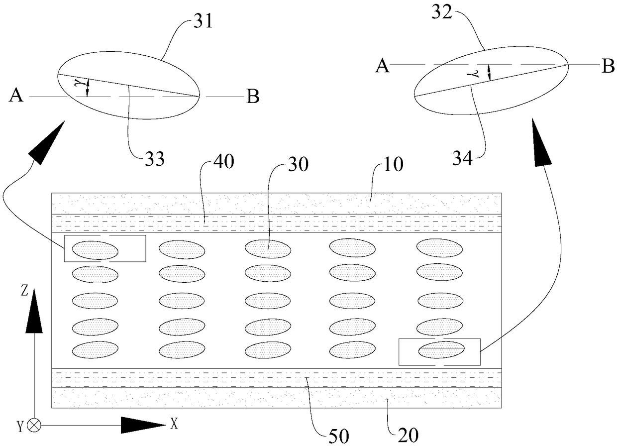
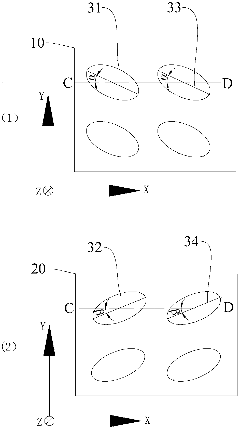
[0035] In one aspect of the invention, the invention provides a display panel. According to an embodiment of the present invention, refer to figure 1 ( figure 1 Among them, the X-axis represents the direction of the long side (or short side) of the display panel, the Z-axis represents the direction of the thickness of the display panel, and the Y-axis represents the direction of the short side (or long ...


PUM

PropertyMeasurementUnit
Amount of delayaaaaaaaaaa

Abstract

The invention provides a display panel and a manufacturing method thereof. The display panel comprises a first substrate, a second substrate, liquid crystal arranged between the first substrate and the second substrate, a first alignment film arranged on the surface, close to the liquid crystal, of the first substrate and a second alignment film arranged on the surface, close to the liquid crystal, of the second substrate, wherein the first substrate and the second substrate which are arranged oppositely, the long axes of liquid crystal molecules respectively close to the first substrate and the second substrate are opposite with respect to the initial inclination direction of the plane where the first substrate is located. Therefore, the difference of liquid crystal delay quantity can bevery well compensated, thus a color castphenomenon is improved, a viewing angle is increased, and the display quality is improved. In addition, a transverse slit electrode can be still adopted, so that the aperture opening ratio of the display panel is not affected.

Description

technical field [0001] The present invention relates to the field of display technology, and in particular, to a display panel, a manufacturing method thereof, and a display device. Background technique [0002] In the existing display panels, the electrodes (common electrodes or pixel electrodes) usually use horizontal slit electrodes (slit electrodes), and the retardation of liquid crystals seen on the left and right sides is different, which will cause color shift and affect the display quality and customer satisfaction. The current improvement solution is to use vertical slit electrodes, but this approach will greatly reduce the aperture ratio. [0003] Therefore, research on improving the difference in retardation of liquid crystals needs to be further studied. Contents of the invention [0004] The present invention aims to solve one of the technical problems in the related art at least to a certain extent. Therefore, an object of the present invention is to propo...

Claims


Application Information

Patent Timeline
06 Nov 2018
Publication
CN108761925A
IPC
G02F1/13363; G02F1/1337
CPC
G02F1/13363; G02F1/133707; G02F1/133784; G02F1/133749; G02F2201/123; G02F2413/02
Inventors
贾倩; 柳在健