Packaging structure and packing method of organic light-emitting diode as well as display device

A technology of light-emitting diodes and packaging structures, which is applied in the direction of organic semiconductor devices, electrical components, and electric solid-state devices. sexual effect

Active Publication Date: 2015-05-27
BOE TECH GRP CO LTD
View PDF4 Cites 11 Cited by
  • Summary
  • Abstract
  • Description
  • Claims
  • Application Information

AI Technical Summary

Problems solved by technology

However, in the non-pixel area, a number of cathode auxiliary lines are arranged on one side of the gate line, signal line and power line, which will lead to a low aperture ratio of the entire display device.
For arranging a number of cathode auxiliary lines on one side of the gate lines, signal lines and power lines, all organic materials need to be evaporated with a fine metal mask (Fine Metal Mask, referred to as FMM) during the evaporation process of organic light-emitting materials. Plating, which increases the difficulty of the evaporation process of organic light-emitting materials, affects efficiency, wastes materials, and brings great difficulties to AMOLED preparation.

Method used


Image

  • Packaging structure and packing method of organic light-emitting diode as well as display device
  • Packaging structure and packing method of organic light-emitting diode as well as display device
  • Packaging structure and packing method of organic light-emitting diode as well as display device

Examples


Embodiment Construction

[0028] The specific embodiments of the invention will be further described below in conjunction with the accompanying drawings. The following examples are only used to illustrate the technical solution of the present invention more clearly, but not to limit the protection scope of the present invention.

[0029] Inorganic films are mainly water and oxygen barrier layers, but they have low elasticity and large internal stress, so flexible packaging cannot be realized. Organic polymers have high elasticity, which can inhibit the cracking of inorganic films and release the stress between inorganic substances. The combination of the two can achieve A flexible packaging method.

[0030] The organic light emitting diode packaging structure in the embodiment of the present invention is based on the above flexible packaging method to realize flexible packaging.

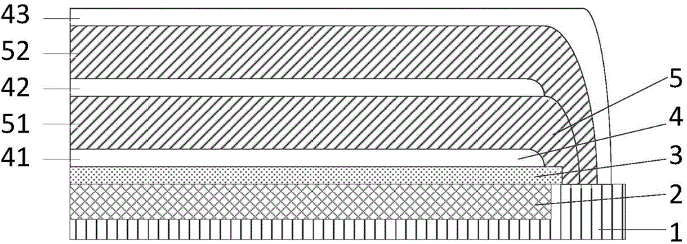
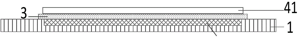
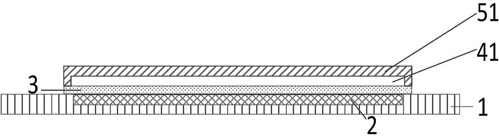
[0031] figure 1 It shows a schematic structural diagram of an organic light emitting diode packaging structure provided b...


PUM


Abstract

The invention discloses a packaging structure and a packing method of an organic light-emitting diode as well as a display device. The packaging structure comprises an organic light-emitting diode display area arranged on a substrate, a cathode pattern arranged on the display area, a first inorganic blocking layer arranged on the cathode pattern, an organic buffering layer positioned on the first inorganic blocking layer and a second inorganic blocking layer, wherein the edge of the organic buffering layer is electrically connected with the cathode pattern on the edge area of the display area; the edge of the second inorganic blocking layer is directly connected with the substrate at the edge area of the display area so as to coat all the other layers. The packaging structure disclosed by the invention has the advantages that since the organic buffering layer is conductive and transparent and the edge of the organic buffering layer is electrically connected with the cathode pattern on the edge area of the display area, the conductivity of the cathode pattern is increased, and furthermore the transmittance of package is not influenced, so that the IR drop is reduced under the condition of guaranteeing simple packaging process and no influence on the opening rate of the display device.

Description

technical field [0001] The invention relates to the field of organic light emitting diode display, in particular to an organic light emitting diode packaging structure and packaging method, and a display device. Background technique [0002] For a top-emitting active matrix organic light emitting diode (Active Matrix Organic Light Emitting Diode, referred to as AMOLED) display device, the cathode is generally made of a conductive metal, such as Mg, Ag and other conductive metals, and is a whole piece covered on the array substrate. Due to the high transparency of the cathode is required for the bulk electrode on the surface, the cathode is usually very thin and the resistance is high. The cathode resistance is very high, which will increase the IR drop (resistance voltage drop). Excessive IR drop will affect the uniformity of the picture. [0003] In the existing solutions, auxiliary cathode lines are used to reduce IR drop, usually in the non-pixel area on the array substr...

Claims


Application Information

Patent Timeline
IPC IPC(8): H01L51/52H01L51/54H01L51/56
CPCH10K50/8445H10K2102/3026H10K50/80H10K50/82H10K71/00H10K71/60H10K2102/101H10K2102/103
Inventor 高静张嵩
Owner BOE TECH GRP CO LTD
Why Eureka
Try Eureka