Top-luminescence organic light-emitting diode (OLED) and preparation method and display apparatus thereof

An electroluminescent device, top-emitting technology, applied in the direction of electro-solid devices, semiconductor/solid-state device manufacturing, electrical components, etc., can solve problems such as large square resistance, reduced current conduction capability, unfavorable electron injection, etc., to reduce square resistance. , Improve the current conduction ability, and ensure the effect of confidentiality

Active Publication Date: 2013-03-27
BOE TECH GRP CO LTD
View PDF3 Cites 10 Cited by
  • Summary
  • Abstract
  • Description
  • Claims
  • Application Information

AI Technical Summary

Problems solved by technology

[0005] In order to realize the top-emitting AM-OLED device, a translucent top electrode is required as the cathode, which is generally made of ultra-thin alloy material, but the ultra-thin alloy material has a large square resistance, which is not conducive to electron injection and will reduce the current flow. Conductivity

Method used


Image

  • Top-luminescence organic light-emitting diode (OLED) and preparation method and display apparatus thereof
  • Top-luminescence organic light-emitting diode (OLED) and preparation method and display apparatus thereof
  • Top-luminescence organic light-emitting diode (OLED) and preparation method and display apparatus thereof

Examples


Embodiment Construction

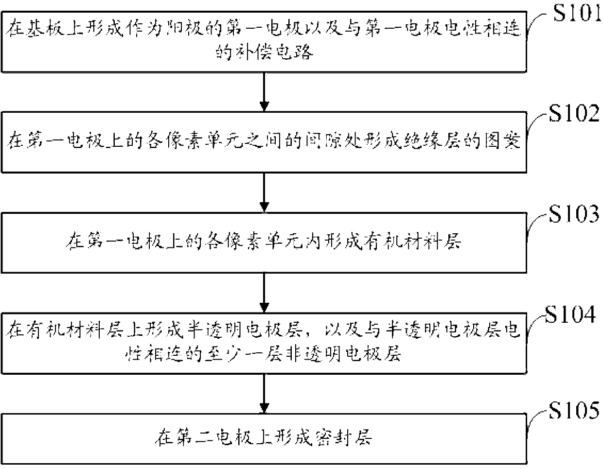
[0022] The specific implementations of the top-emission organic electroluminescent device, its manufacturing method and display device provided by the embodiments of the present invention will be described in detail below with reference to the accompanying drawings.

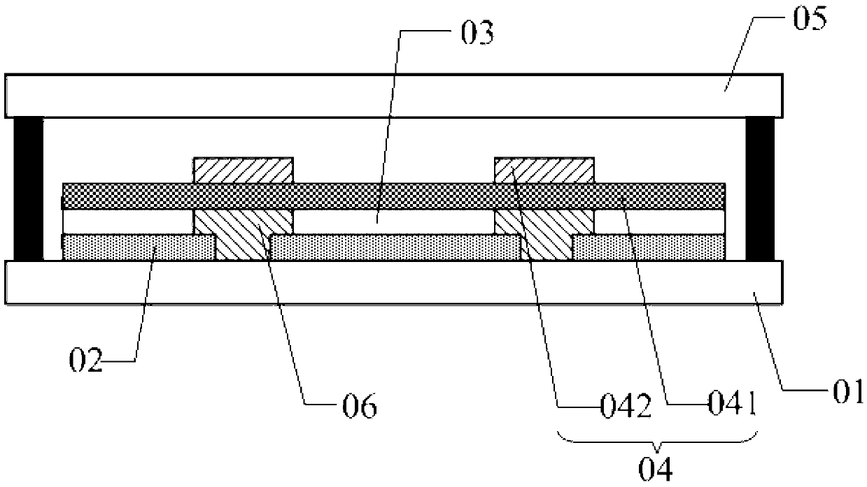
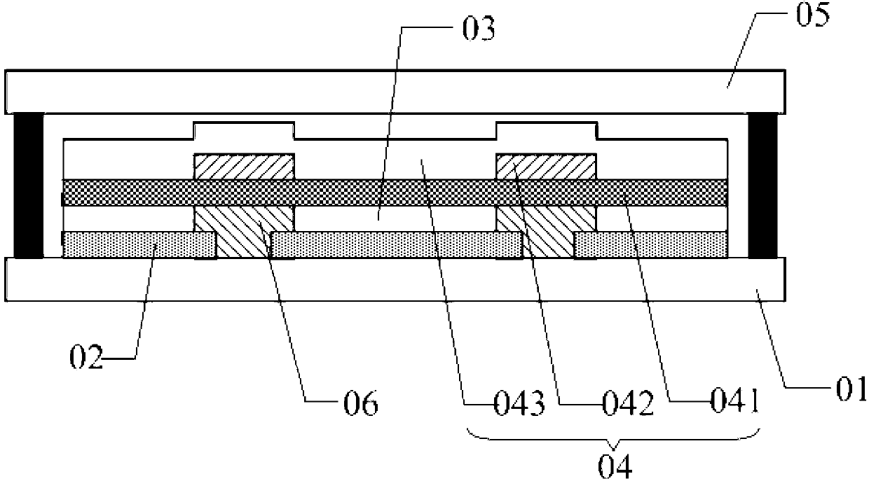
[0023] The film thickness and shape of each layer in the drawings do not reflect the true scale of the OLED device, but are only intended to schematically illustrate the content of the present invention.

[0024] A top-emission organic electroluminescent device provided by an embodiment of the present invention, such as figure 1 As shown, the substrate 01 is included, and the substrate 01 has a first electrode 02 as an anode, an organic material layer 03, a second electrode 04 as a cathode, and a sealing layer 05 on the substrate 01 from bottom to top, wherein the second electrode 04 specifically includes :

[0025] A semi-transparent electrode layer 041, and at least one non-transparent electrode layer 042 elec...


PUM

PropertyMeasurementUnit
Thicknessaaaaaaaaaa
Thicknessaaaaaaaaaa

Abstract

The invention discloses a top-luminescence OLED and a preparation method and a display apparatus thereof. A second electrode serving as a cathode in the OLED is composed of a semitransparent electrode layer and at least one non-transparent electrode layer electrically connected with the semitransparent electrode layer. Patterns arranged on the at least one non-transparent electrode layer right face gaps among determined pixel units of an organic material layer, so that the aperture opening ratio of the OLED is not affected; and the at least one non-transparent electrode layer electrically connected with the semitransparent electrode layer can reduce the square resistance of the semitransparent electrode layer, so that the current conduction capacity of the cathode of the OLED is improved. Further, the display perspective of the OLED can be controlled effectively by designing the patterns of the at least one non-transparent electrode layer, so that pictures can be viewed at specific angles, and the display security is guaranteed.

Description

technical field [0001] The invention relates to the field of display technology, in particular to a top-emission organic electroluminescence device, a preparation method thereof and a display device. Background technique [0002] In the field of optoelectronic display technology, Organic Light Emitting Diode (OLED) has many advantages such as active light emission, high brightness, high contrast, ultra-thin, low power consumption, large viewing angle and wide operating temperature range. Advanced new flat panel display device. [0003] OLED is a multi-film laminated structure. Several layers of organic material layers are sandwiched between a pair of electrodes. When an appropriate voltage is applied, electrons and holes are injected from the corresponding electrodes into the organic material layer. The corresponding positions meet and recombine, release energy and emit light. [0004] In the active AM-OLED, a thin film transistor is arranged in each pixel unit to control ...

Claims


Application Information

Patent Timeline
IPC IPC(8): H01L51/50H01L51/52H01L51/56
Inventor 王玉林于军胜
Owner BOE TECH GRP CO LTD
Why Eureka
Try Eureka