
Manufacturing method of high-density interconnected thick copper plate and thick copper core plate

A technology of high-density interconnection and manufacturing method, which is applied in the field of circuit board production and manufacturing, can solve the problems of white spots in copper-free areas and delamination of high-density interconnection thickness boards, and achieve the effect of avoiding white spots and delamination.

Inactive Publication Date: 2018-11-13
GUANGZHOU FASTPRINT CIRCUIT TECH +2
View PDF3 Cites 0 Cited by
  • Summary
  • Abstract
  • Description
  • Claims
  • Application Information

AI Technical Summary

Problems solved by technology

However, when thick copper core boards are laminated to obtain high-density interconnected thick boards, white spots often appear in the copper-free areas of high-density interconnected thick boards, and it is easy to cause delamination of high-density interconnected thick boards

Method used

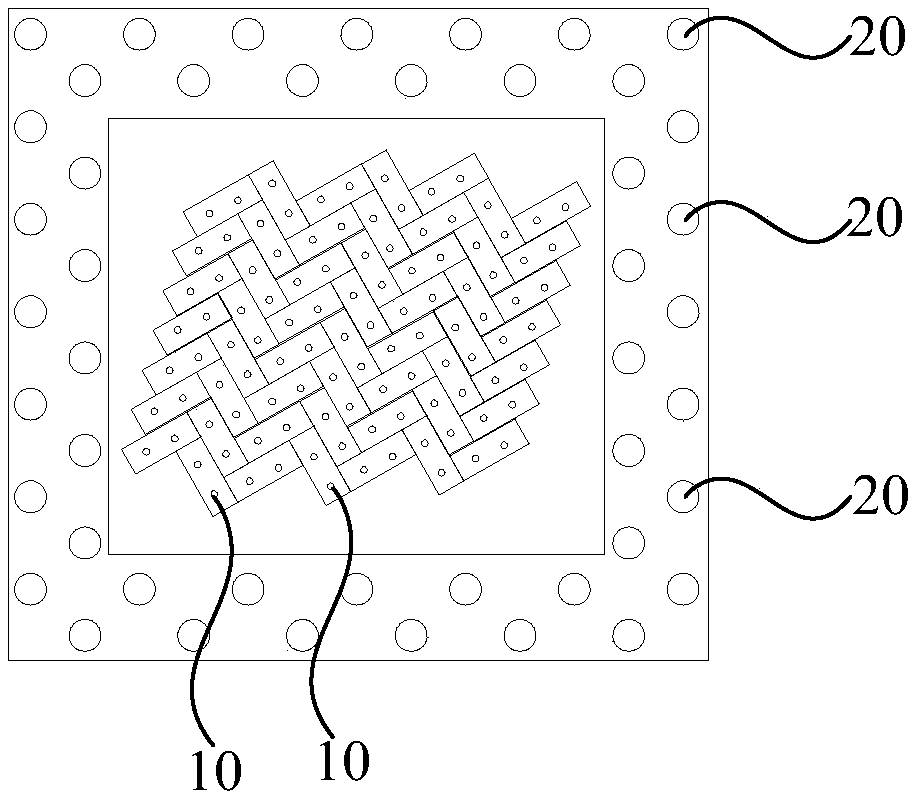
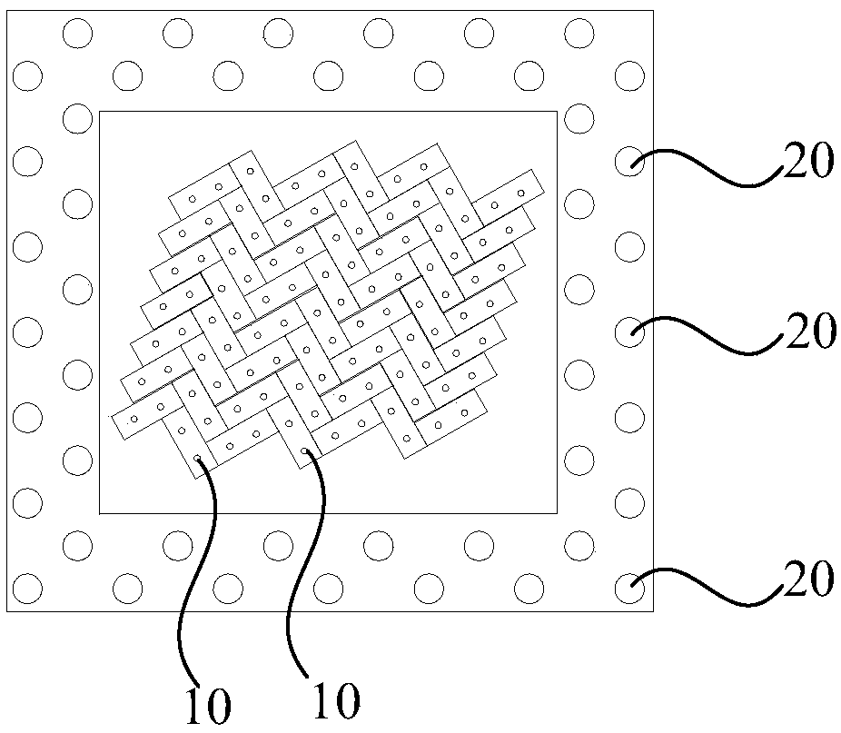

Image

  • Manufacturing method of high-density interconnected thick copper plate and thick copper core plate
  • Manufacturing method of high-density interconnected thick copper plate and thick copper core plate

Examples


Embodiment Construction

[0022] In order to make the above objects, features and advantages of the present invention more comprehensible, specific implementations of the present invention will be described in detail below in conjunction with the accompanying drawings. In the following description, numerous specific details are set forth in order to provide a thorough understanding of the present invention. However, the present invention can be implemented in many other ways different from those described here, and those skilled in the art can make similar improvements without departing from the connotation of the present invention, so the present invention is not limited by the specific embodiments disclosed below.

[0023] In the description of the present invention, it should be understood that the terms "first" and "second" are used for description purposes only, and cannot be interpreted as indicating or implying relative importance or implicitly indicating the quantity of indicated technical featu...


PUM

PropertyMeasurementUnit
diameteraaaaaaaaaa

Abstract

The invention relates to a manufacturing method of a high-density interconnected thick copper plate and a thick copper core plate. The method comprises the following steps: determining preset positions of to-be-machined heat dissipation holes in the thick copper core plate before the thick copper core plate is laminated, and performing manufacturing at the preset positions of the thick copper coreplate to obtain a copper disk; laminating two or more of the thick copper core plates with the copper disks through prepreg to obtain a laminate; machining heat dissipation holes in the laminate in positions corresponding to the preset positions, and removing the copper disks in the preset positions of the thick copper core plates in the process of machining the heat dissipation holes. Accordingto the manufacturing method of the high-density interconnected thick copper plate, since the copper disks are manufactured in the preset positions of the to-be-machined heat dissipation holes in the thick copper core plate, the residual copper rate of the thick copper core plate is increased. During lamination, stress on a base material in copper-free areas on the thick copper core plate can be increased by the copper disks, so that glue filling fluidity in the copper-free areas is better, the copper-free areas can be fully filled, and white spots and delamination can be avoided.

Description

technical field [0001] The invention relates to the technical field of circuit board production and manufacturing, in particular to a method for manufacturing a high-density interconnect thick copper board and a thick copper core board. Background technique [0002] In order to meet the requirements of fast signal transmission and easy heat dissipation, high-density interconnection boards are often laminated with multiple thick copper core boards with a surface copper thickness ≥ 2OZ to obtain high-density interconnection thickness boards. However, when the thick copper core board is laminated to obtain the high-density interconnected thick board, white spots often appear in the copper-free area of ​​the high-density interconnected thick board, and it is easy to cause delamination of the high-density interconnected thick board. Contents of the invention [0003] Based on this, it is necessary to overcome the defects of the prior art and provide a method for manufacturing h...

Claims


Application Information

Patent Timeline
Patent Type & Authority Applications(China)
IPC IPC(8): H05K3/46H05K1/02
CPCH05K3/4611H05K1/0206H05K3/4638
Inventor 吴辉陈黎阳罗畅
Owner GUANGZHOU FASTPRINT CIRCUIT TECH
Learn More