Touch display substrate and its preparation method, repair method, touch display panel

A technology for touch display substrates and touch leads, which is applied in the fields of instruments, computing, and electrical digital data processing, etc., and can solve problems such as poor touch electrodes, dark touch leads and data lines, short circuits between touch leads and data lines, etc. problems, to achieve the effect of eliminating short circuit problems, eliminating dark line defects, and improving the yield rate

Active Publication Date: 2022-02-25
BOE TECH GRP CO LTD +1
View PDF0 Cites 0 Cited by
  • Summary
  • Abstract
  • Description
  • Claims
  • Application Information

AI Technical Summary

Problems solved by technology

[0004] The same-layer structure of touch leads and data lines is generally called a dual source (Dual source) structure. Although it has the advantages of less number of patterning processes and low production costs, because the touch leads and data lines are arranged on the same layer and adjacent to each other, additional The problem of short circuit between the touch lead and the data line, and the short circuit between the touch lead and the data line will cause poor dark lines and poor touch electrodes

Method used


Image

  • Touch display substrate and its preparation method, repair method, touch display panel
  • Touch display substrate and its preparation method, repair method, touch display panel
  • Touch display substrate and its preparation method, repair method, touch display panel

Examples


no. 1 example

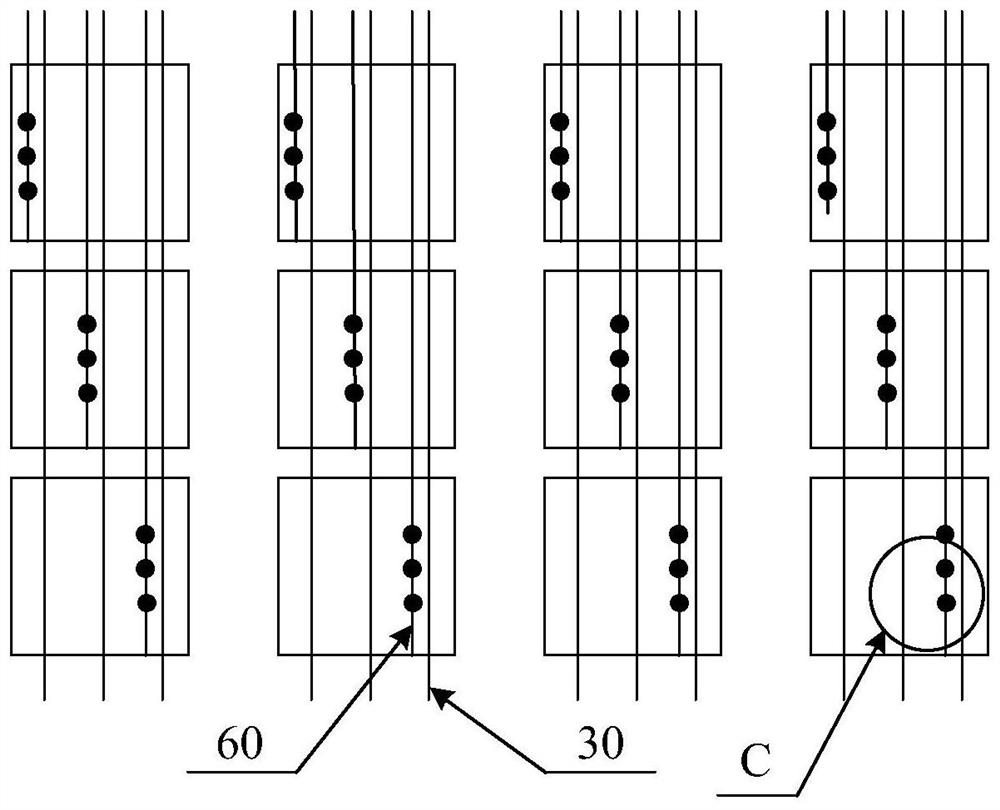
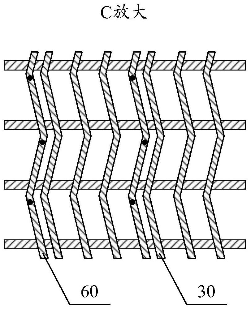
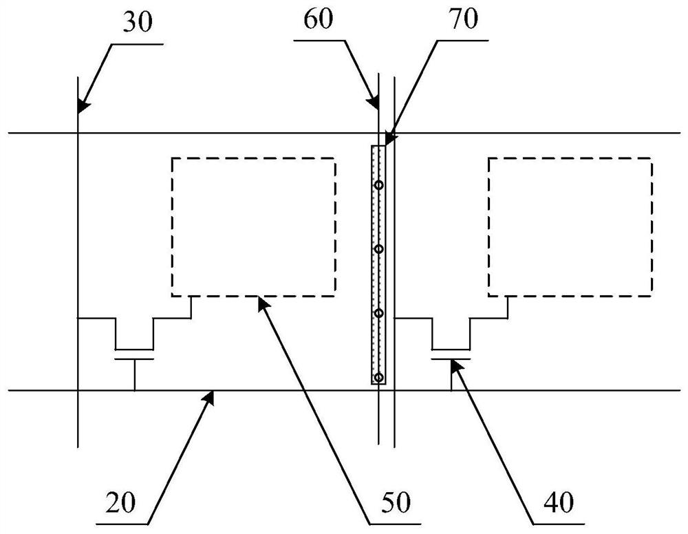
[0049] The main structure of the touch display substrate in this embodiment includes gate lines, data lines, thin film transistors, pixel electrodes, touch leads and connection lines. The gate lines and data lines vertically intersect to define several pixel units, and the thin film transistors and pixel electrodes are arranged on In each pixel unit, the touch wires are arranged between adjacent pixel units and connected to the touch electrodes. In this embodiment, the connection lines and the gate lines are arranged on the same layer and formed by the same patterning process, and a plurality of connection vias are opened on the first insulating layer covering the gate lines and the connection lines, and the touch leads pass through the plurality of connection vias. The hole is connected with the connecting wire.

[0050] The technical solution of this embodiment will be further described below through the preparation process of the touch display substrate.

[0051] Figure ...

no. 2 example

[0071] The main structure of the touch display substrate in this embodiment is the same as that of the aforementioned first embodiment, including gate lines, data lines, thin film transistors, pixel electrodes, touch leads and connection lines, and the gate lines and data lines vertically intersect to define several pixel units , the thin film transistor and the pixel electrode are arranged in each pixel unit, and the touch lead is arranged between adjacent pixel units and connected with the touch electrode. Different from the bottom gate structure in the first embodiment, the embodiment of the present application is a top gate structure.

[0072] The manufacturing process of the touch display substrate in this embodiment includes: firstly, a shielding layer and an active layer pattern are formed on the substrate through a patterning process. Subsequently, a first insulating layer is deposited, and patterns of gate electrodes, gate lines and connecting lines are formed on the ...

no. 3 example

[0083] Based on the technical concept of the present invention, the technical solutions of the foregoing embodiments can also be expanded in various aspects. As an implementation solution, the connecting wires may be arranged in other film layers, not necessarily in the same layer as the grid lines, for example, may be arranged in the same layer as the shielding layer. As another implementation solution, the connection wires can be arranged in the film layer above the touch lead wires and data lines, that is, the connection wires are arranged in a film layer far away from the base relative to the film layer where the touch lead wires and data lines are located. Touch leads can be cut from the backside of the substrate. As yet another implementation solution, the connecting wires can be separately arranged in one film layer and prepared through a single patterning process. Other extensions The present invention is not specifically limited here, and the above extensions can eff...


PUM


Abstract

The invention provides a touch display substrate, a preparation method thereof, a repair method, and a touch display panel. The touch display substrate includes a plurality of pixel units defined by gate lines and data lines, as well as touch wires arranged between adjacent pixel units and connecting wires as redundant touch wires, the touch wires pass through multiple The connecting vias are connected with the connecting wires. The repair method includes: after locating the short-circuit point, respectively determining the first connection via hole and the second connection via hole on both sides of the short-circuit point; Connect the touch leads between the vias. In the present invention, by setting the connecting wire as a redundant touch lead, and the connecting wire and the touch lead are connected through a plurality of connection vias, it can effectively eliminate the dark wire defect and the touch electrode defect caused by the short circuit of the touch lead and the data line. Improve the yield rate.

Description

technical field [0001] The invention relates to the field of display technology, in particular to a touch display substrate, a preparation method thereof, and a repair method thereof. Background technique [0002] With the rapid development of display technology, touch panels (Touch Panel) have gradually spread in people's lives. Touch panels can be classified into add-on mode (Add on Mode), surface-covering type (On Cell), embedded type (InCell) and the like according to the composition structure. Among them, the embedded touch panel is to embed the touch electrodes of the touch module inside the display module, and combine the display and touch into one, which not only greatly reduces the overall thickness of the module, but also makes the product lighter and thinner, and greatly The production cost is reduced. Among them, in the embedded touch panel, touch and display driver integration (Touch and Display Driver Integration, TDDI) as a new technology, due to its thin an...

Claims


Application Information

Patent Timeline
Patent Type & Authority Patents(China)
IPC IPC(8): G06F3/041
CPCG06F3/0412
Inventor 张伟张文龙
Owner BOE TECH GRP CO LTD
Why Eureka
Try Eureka