Pixel circuit, drive method therefor, display panel, and splicing screen
A technology of a pixel circuit and a driving method, applied in the display field, can solve the problems of main wave peak shift, narrow frame of signal lines, etc., and achieve the effect of reducing wiring, realizing narrow frame design, and realizing large-size and high-resolution panels.
- Summary
- Abstract
- Description
- Claims
- Application Information
AI Technical Summary
Problems solved by technology
Method used
Image


Examples
Embodiment 1
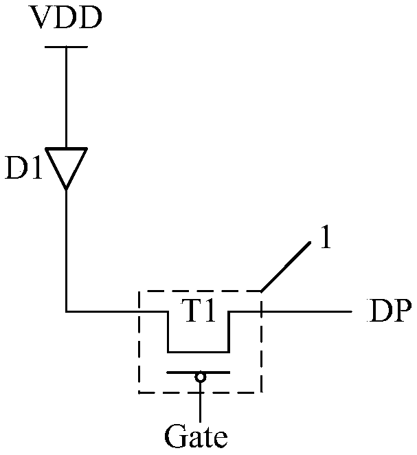
[0046] combine figure 1 As shown, this embodiment provides a pixel circuit, including: a light-emitting diode D1 and a switch unit 1, wherein the light-emitting diode D1 has an anode and a cathode, the anode of the light-emitting diode D1 is used to receive the first power supply voltage, and the switch unit 1 responds Based on the scanning signal, under the control of the display control signal, the second power supply voltage received by the cathode of the light emitting diode D1 is controlled to control the light emitting state of the light emitting diode D1.
[0047] Since the switch unit 1 is added to the pixel circuit in this embodiment, when the pixel circuit in this embodiment is applied to a display panel, the switch unit 1 in the pixel circuit in the same row can be connected to the same scanning line Gate , connect the switch units 1 of the pixel circuits in the same column to the same display signal line DP. In this way, by inputting the scanning signal to the sca...
Embodiment 2
[0059] to combine figure 2 As shown, this embodiment provides a pixel circuit, including: a switching transistor T1, a light emission control transistor T2, a reset transistor T3, and a light emitting diode D1; wherein, the source of the switching transistor T1 is connected to the display signal line DP, and the drain is connected to the light emitting diode The cathode of D1, the gate is connected to the scan line Gate; the source of the light-emitting control transistor T2 is connected to the cathode of the light-emitting diode D1, the drain is connected to the second power supply voltage terminal VSS, and the gate is connected to the drain of the switching transistor T1; the source of the reset transistor T3 The pole is connected to the reset signal line VGH, the drain is connected to the cathode of the light-emitting diode D1, and the gate is connected to the reset signal line DN; the source of the light-emitting diode D1 is connected to the first power supply voltage term...
Embodiment 3
[0068] Such as Figure 4 As shown, this embodiment provides a display panel, including a plurality of display signal lines (DP1-DPm), a plurality of reset signal lines (DN1-DNn), and a plurality of scanning lines (Gate1-Gaten); wherein, a plurality of Display signal lines (DP1-DPm) and a plurality of scanning lines (Gate1-Gaten) are intersected, and pixel circuits are arranged at the intersecting positions; the pixel circuits may be the pixel circuits in Embodiment 1 or 2. Wherein, the switch units 1 in the pixel circuits in the same row are connected to the same scan line Gate, and the switch units 1 in the pixel circuits in the same column are connected to the same display signal line DP.
[0069] In the display panel of this embodiment, the switch units 1 in the pixel circuits in the same row are connected to the same scan line Gate, and the switch units 1 in the pixel circuits in the same column are connected to the same display signal line DP. In this way, through Input ...
PUM
 Abstract
Description
Claims
Application Information