
Memory control chip, memory device, and adaptive interface method

A storage control and chip technology, applied in the field of storage devices and self-adaptive interfaces, and storage control chips, can solve problems such as variable length, complex connection lines of storage devices, affecting high-speed signal timing and anti-interference, and achieve simple connection lines Effect

Active Publication Date: 2018-12-11
SHENZHEN NETCOM ELECTRONICS CO LTD
View PDF7 Cites 0 Cited by
  • Summary
  • Abstract
  • Description
  • Claims
  • Application Information

AI Technical Summary

Problems solved by technology

like figure 1 and figure 2 As shown, the storage device 1 includes a first memory 01, a second memory 02, and a controller 03. The first memory 01 and the second memory 02 are respectively connected to the controller 03. Since the placement positions are opposite, the pins on the first memory 01 The order of I / O0-I / O7 is opposite to the order of the pins I / O0-I / O7 on the second memory 02, so that the connection lines between the second memory 02 and the controller 03 are crossed, thereby increasing the printing speed. Difficulty in board layout, and longer traces affect timing and noise immunity of high-speed signals
[0004] In the process of implementing the embodiments of the present invention, the inventors found that the connection lines of the storage devices in the prior art are complicated, which further affects the performance of the storage devices

Method used


Image

  • Memory control chip, memory device, and adaptive interface method
  • Memory control chip, memory device, and adaptive interface method
  • Memory control chip, memory device, and adaptive interface method

Examples


Embodiment Construction

[0033] In order to make the object, technical solution and advantages of the present invention clearer, the present invention will be further described in detail below in conjunction with the accompanying drawings and embodiments. It should be understood that the specific embodiments described here are only used to explain the present invention, not to limit the present invention.

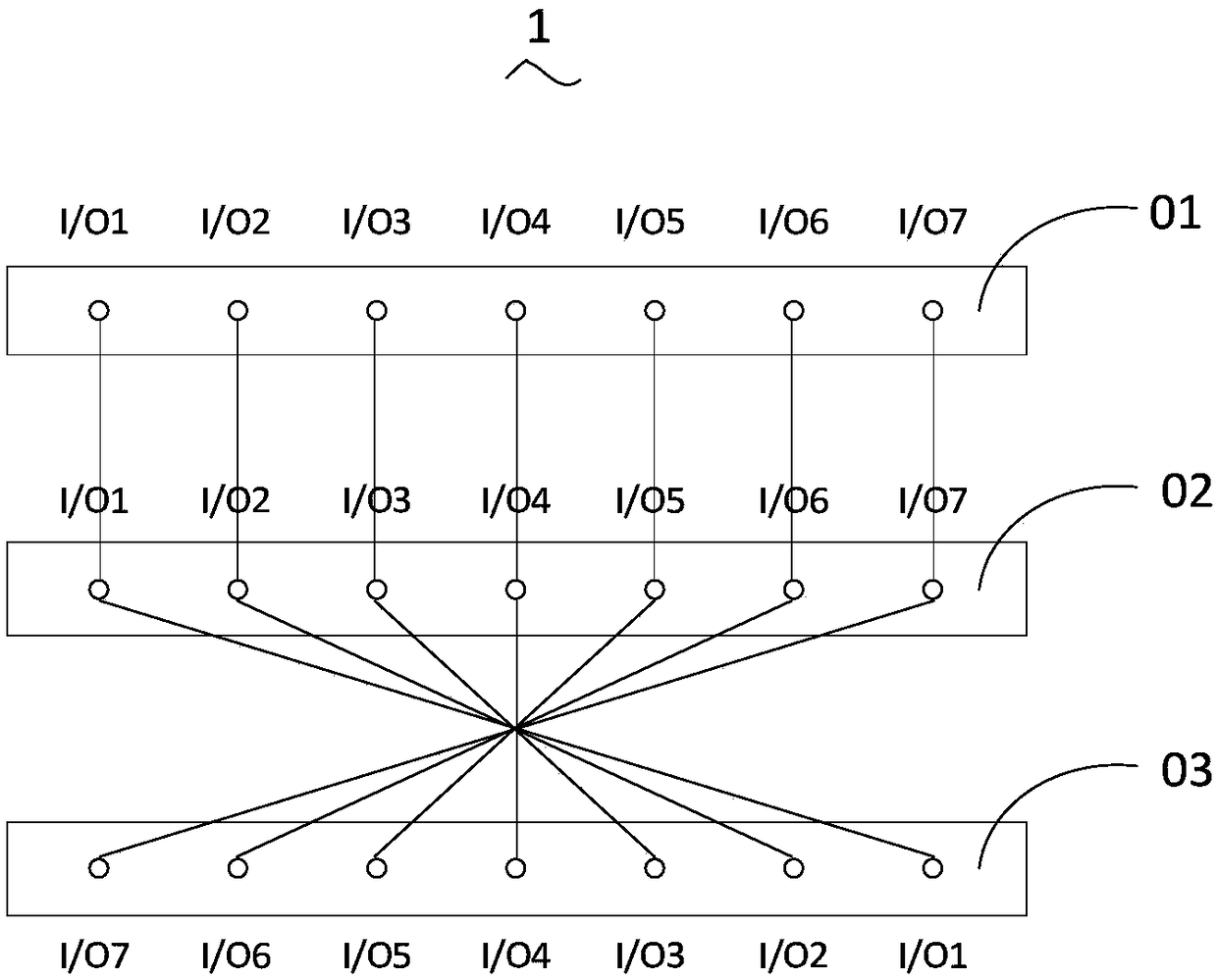
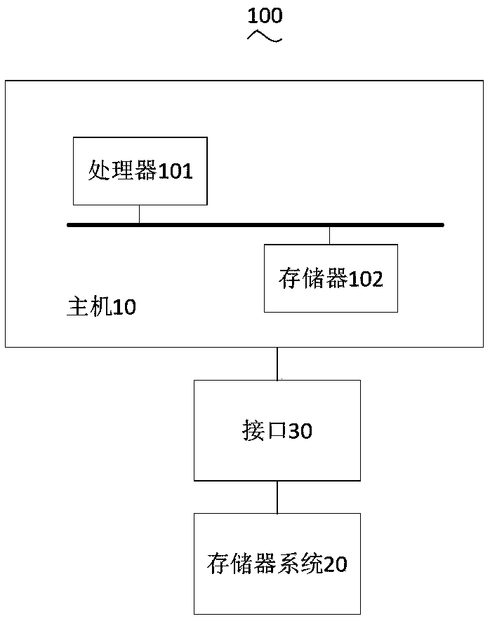
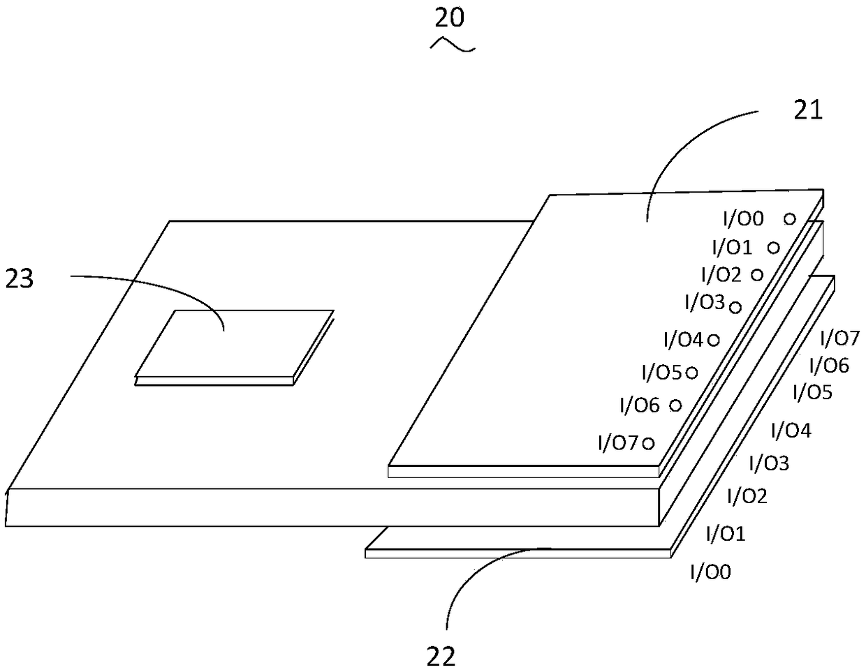
[0034] The present invention includes a storage control chip, a storage device, and an adaptive interface method, wherein the storage control chip is connected to the first memory and the second memory, and the storage control chip includes: an interface circuit, respectively connected to the first memory, the second memory, The second memory is connected to a function selection circuit, connected to the interface circuit, for selecting the interface function of the interface circuit; a controller, connected to the interface circuit, and connected to the function selection circuit through the interf...


PUM


Abstract

The invention relates to the technical field of chips, and discloses a memory control chip, a memory device and an adaptive interface method. The memory control chip is connected with a first memory and a second memory. The memory control chip includes: an interface circuit for connecting with the first memory and the second memory; a function selection circuit connected to the interface circuit for selecting an interface function of the interface circuit; a controller, which is y connected with the interface circuit and the function selection circuit for configuring the state of the interfacecircuit and controlling the function selection circuit to select the interface function. In the above manner, the embodiment of the present invention can simplify the connection line of the memory device.

Description

technical field [0001] The invention relates to the field of chip technology, in particular to a storage control chip, a storage device and an adaptive interface method. Background technique [0002] Storage devices include U disk (USB flash disk, USB flash disk), SSD, emmc, EMCP, ufs, SD card and other devices, which are widely used in various products, such as computers, mobile phones and other electronic products. As the functions of electronic products become more and more abundant, and the volume is becoming thinner and smaller, this puts forward higher requirements for the structure of the internal circuit board of the storage device. [0003] In the design of the circuit board, when the placement operation needs to be performed on both sides of the circuit board, the problem of the definition order of the pins will be encountered. like figure 1 and figure 2 As shown, the storage device 1 includes a first memory 01, a second memory 02, and a controller 03. The firs...

Claims


Application Information

Patent Timeline
IPC IPC(8): G11C7/10
CPCG11C7/1048
Inventor 邓恩华郭丹
Owner SHENZHEN NETCOM ELECTRONICS CO LTD
Learn More