touch panel
A touch panel and touch area technology, applied in the field of touch technology, can solve the problems of increased electrode signal, incomplete coverage of electrodes, uneven distribution of capacitance, etc., and achieve the effect of uniform distribution of capacitance
- Summary
- Abstract
- Description
- Claims
- Application Information
AI Technical Summary
Problems solved by technology
Method used
Image
Examples
Embodiment Construction
[0032] Please refer to the drawings in the accompanying drawings, wherein like reference numerals refer to like components. The following description is based on illustrated specific embodiments of the present application, which should not be construed as limiting other specific embodiments of the present application that are not described in detail here.
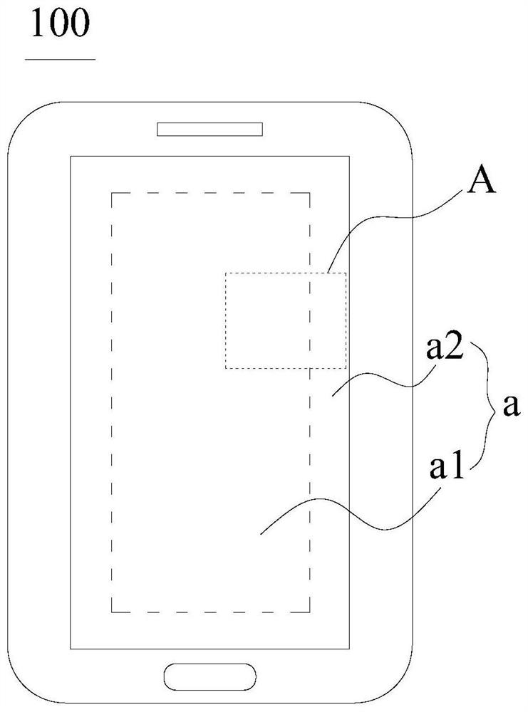
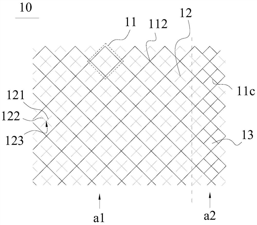
[0033] Please refer to figure 2 and image 3 , figure 2 It is a schematic structural diagram of the first embodiment of the touch panel of the present application; image 3 for figure 2 Enlarged view of A. In the first embodiment of the touch panel of the present application, the touch panel 100 includes a substrate 13 and a touch area a disposed on the substrate 13 . The touch area a includes a metal grid structure 10 . The metal grid structure 10 includes a plurality of unit grids 11 and dummy units 12 .
[0034] A plurality of unit grids 11 are connected to each other. The dummy cell 12 includes at least one f...
PUM
 Abstract
Description
Claims
Application Information


